Atomic Force Microscopy (AFM) remains a cornerstone technique in nanoscience, enabling high-resolution imaging and manipulation at the nanoscale.
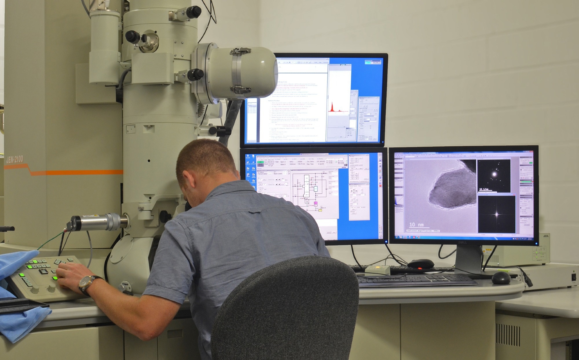 Image Credit: Rui Serra Maia/Shutterstock.com
As of early 2026, the global AFM market has expanded to approximately USD 542 million, up from USD 514 million in 2024, reflecting increased demand from semiconductor fabrication, nanotechnology research, and advanced life science applications.1
This report includes preliminary data through Q1 2026, with a focus on recent technical advances and major industry participants, including Bruker, Nanosurf, and CSInstruments.
Saving this article for later? Download a PDF here.
Applying Atomic Force Microscopy to Nanoscience
AFM works by raster-scanning a fine probe over a sample surface, and laser diffraction detects minute variations in the probe's height. This data is then mapped into topographical images with nanometer-scale resolution far surpassing the diffraction limit of optical microscopy.2
This contact-based technique is especially effective for characterizing surface roughness, measuring nanoparticle dimensions, and analyzing nanostructures such as carbon nanotubes. It also requires less sample preparation than electron microscopy and works well across a wide range of materials, from rigid metals to soft biomolecules.2
AFM has been particularly powerful in advancing nanoscience: it can detail a material's 3D topography, mechanical properties (e.g., stiffness via PeakForce Tapping), and even its electrical and chemical properties. It is used in a range of applications:
- Semiconductors (defect detection on wafers)
- Electronics (e.g., 2D materials like graphene)
- Biomedicine (protein mapping)
Its non-destructive nature supports iterative R&D, accelerating innovations in quantum devices, energy storage, and drug delivery that are critical as device nodes shrink below 2 nm. Industrial adoption now exceeds academia, with quality control in chip fabs boosting yields and reducing defects.3
Recent Developments in AFM
In recent years, AFM has moved from a useful lab tool to an industrialized machine. High-speed systems like Bruker's Dimension Nexus (launched Dec 2024) and Park Systems' FX300 (Feb 2025) achieve 1,250 lines/sec and 45 fps, enabling real-time dynamic imaging of processes like self-assembly or etching that were previously impossible.
Oxford Instruments' Jupiter Discovery (May 2025) targets large samples with intuitive interfaces for multi-user facilities 1, 4
Multimodal integration proliferates: platforms combining AFM with STM, Raman, and microwave microscopy (e.g., PrimeNano's Scanwave Pro) deliver holistic nanomaterial profiles of topography plus electronics. AI/ML enhancements automate analysis, defect detection, and adaptive scanning, addressing throughput limits.4
Non-contact and PeakForce modes mitigate sample damage, which is vital for soft-matter-like cells or polymers. Cryogenic/high-magnetic AFMs (e.g., Attocube) probe superconductors and quantum materials. These innovations, fueled by $2.2B US NNI funding in 2025, expand AFM into OLED production and battery R&D.4
Current Global Market of AFM
The global atomic force microscopy (AFM) market reached USD 541.8 million in 2025 and is projected to reach USD 762.2 million by 2030, reflecting a compound annual growth rate (CAGR) of 7.1 %, according to MarketsandMarkets. This forecast aligns closely with Coherent Market Insights' assessment of USD 632.6 million in 2025, rising to USD 890.7 million by 2032 at a 5.0 % CAGR.5
The Asia-Pacific region holds the dominant market share of 47.3 %, driven by semiconductor manufacturing centers in Taiwan, South Korea, Japan, and China's strategic nanotechnology initiatives; North America accounts for approximately 38 %, while Europe maintains a smaller but innovation-led position.1
Industrial-grade AFMs command the largest segment share with a 7.5 % CAGR, surpassing research-grade systems due to demand for precision metrology in semiconductors and electronics, the fastest-growing application at over 7 % CAGR and 34.7 % share. Materials science/nanotechnology and life sciences follow as key applications.5
Post-COVID-19 recovery has been robust, with companies such as Oxford Instruments and Horiba reporting sales growth that exceeded pre-pandemic levels despite temporary 2021 setbacks. Growth in probes and software segments is fuelled by specialized offerings, including conductive tips for electrical characterization.1, 5
| Market Segment |
2025 Share/Size (USD Mn) |
CAGR to 2030 |
| Industrial Grade |
Largest (~62 %) |
7.5 % |
| Semis & Electronics |
34.7 % |
>7 % |
| Asia-Pacific |
47.30 % |
Fastest |
| Probes/Software |
Growing |
7 %+ |
Lingering challenges include high instrument costs limiting small- and medium-sized enterprise adoption, potential sample damage from contact modes, and scan speed constraints on throughput. Nevertheless, substantial forces – such as the European Union's €1 billion Horizon Europe nanotechnology investments – sustain market momentum.5
Major Players in the AFM Industry
Bruker (USA), a market leader with over 4,600 Dimension-series systems installed globally, offers the Dimension Icon, Icon NXT, and the newly launched Dimension Nexus (December 2024).
The Nexus uses the NanoScope 6 controller and Bruker’s PeakForce Tapping technology, supporting more than 50 modes for nanomechanical and electrical mapping in semiconductor and life science research. Its low-drift design and straightforward interface are intended to support higher throughput in multi-user lab settings.6
Park Systems (South Korea), another prominent player in high-resolution metrology, offers the FX40 (2021) and the updated FX300 IR (2025 expansion). The FX300 IR automates analysis of up to 300 mm wafers, integrating Photo-induced Force Microscopy (PiFM) and infrared spectroscopy for chemical imaging and quality control in semiconductors, with features like sliding/rotation stages and cleanroom compatibility.7
Nanosurf AG (Switzerland) specializes in compact, accessible AFMs for academia and industry, including the DriveAFM, FlexAFM, and CoreAFM lines. The DriveAFM uses direct-drive piezo actuation for ultra-low noise and high-bandwidth imaging of nanostructures, proteins, and polymers, emphasizing custom modes and ease of use.8
Oxford Instruments - Asylum Research (UK), strengthened by the 2021 WITec acquisition, delivers innovative systems, including the Cypher VRS1250 and the Cypher ES Battery Edition (enhanced in 2024). The ES Battery Edition supports video-rate imaging of electrode/electrolyte interfaces in batteries and 2D materials, enabling optimization of solid-electrolyte interphases (SEIs) and electrical double layers.9
CSInstruments (France) is a manufacturer of Atomic Force Microscopes, specializing in the Nano-Observer AFM and Galaxy Controller product lines. Its AFM systems are designed for nano-R&D applications, including 2D materials characterization, conductive AFM (C-AFM), and various scanning probe techniques. The company also offers probes and accessories compatible with other manufacturers’ systems.10
Other notables include Hitachi High-Tech (AFM5300E vacuum series for air/liquid/vacuum/humidity/temperature control from -120°C to 800°C), Horiba (AFM-Raman platforms like NanoRaman for co-localized measurements), and Semilab (emerging in semiconductor metrology). Startups such as GeTec and Molecular Vista target subsurface and niche imaging.5
|
Headquarters |
Key Products (Recent) |
Market Strength |
| Bruker |
USA |
Dimension Nexus (2024) |
Leader in modes/versatility |
| Park Systems |
South Korea |
FX300 IR (2025) |
Wafer metrology/spectroscopy |
| Nanosurf |
Switzerland |
DriveAFM |
Compact/high-res imaging |
| Oxford Instruments |
UK |
Cypher ES Battery (2024) |
Academic and industry R&D |
| CSInstruments |
France |
Specialty probes |
Compact AFMs for nano-R&D |
Future Directions for AFM
Looking ahead to 2030, AFM is expected to move further toward AI-guided, multimodal platforms designed for industrial nanofabrication. Advances in probe design could push resolution even closer to the sub-atomic scale, while imaging speeds above 100 frames per second and integrated cryogenic and liquid-mode capabilities would broaden the technique’s usefulness across both research and production settings.5
Much of this progress will be shaped by semiconductor manufacturing, where continued scaling toward sub-3 nm nodes is driving demand for more precise and adaptable nanoscale characterization. At the same time, research on batteries and OLEDs is creating new opportunities for quantitative imaging methods that measure properties such as adhesion and stiffness.
Continued improvements in PeakForce and QI-based approaches are also likely to expand AFM’s role in biomedicine, while more specialized systems are being developed for quantum and 2D materials research.3
Several factors are helping support this transition, including lower-cost MEMS-based components, cloud-based AI analysis, and the wider adoption of inline quality assurance standards. Asia-Pacific is likely to strengthen its lead and account for more than half of the global market, even as consolidation continues through deals such as Oxford Instruments’ acquisition of WITec.1
At the same time, throughput continues to be a practical constraint, particularly as AFM takes on a larger role in a nano-enabled economy valued at more than USD 100 billion.1
Learn how AFM is used in semiconductor manufacturing here.
An Ever-Evolving Technology
AFM’s progress is increasingly being shaped by how closely advances in probes, detectors, and software can be integrated into a single measurement platform.
Newer developments, like self-sensing cantilevers and machine-learning-assisted analysis, are improving sensitivity, streamlining operations, and extending the technique’s usefulness across both research and industrial settings.
References and Further Readings
- Atomic Force Microscopy Market Size, Share & Trends. https://www.marketsandmarkets.com/Market-Reports/atomic-force-microscopy-market-57704156.html.
- VD dos Santos, A. C.; Hondl, N.; Ramos-Garcia, V.; Kuligowski, J.; Lendl, B.; Ramer, G., AFM-IR for nanoscale chemical characterization in life sciences: recent developments and future directions. ACS measurement science au 2023, 3 (5), 301-314.
- Khan, W. S.; Asmatulu, E.; Asmatulu, R., Nanotechnology emerging trends, markets and concerns. In Nanotechnology safety, Elsevier: 2025; pp 1-21.
- Wei, X.; Jia, L.; Duan, B.; Wang, X.; Du, L.; Li, S.; Xu, Z.; Zhao, W., Recent progress and applications of nanoIR-AFM in morphological characterization of organic solar cells. Advanced Functional Materials 2024, 34 (49), 2408960. DOI:10.1002/adfm.202408960, https://onlinelibrary.wiley.com/doi/10.1002/adfm.202408960.
- Atomic Force Microscopy (AFM) Research Report 2026 - Global $707.22 Mn Market Trends, Opportunities, and Forecasts to 2031. https://www.globenewswire.com/news-release/2026/01/30/3229321/28124/en/Atomic-Force-Microscopy-AFM-Research-Report-2026-Global-707-22-Mn-Market-Trends-Opportunities-and-Forecasts-to-2031.html. [Accessed March 2026]
- Bruker Introduces Dimension Nexus™ Atomic Force Microscope. https://www.bruker.com/en/news-and-events/news/2024/bruker-introduces-dimension-nexus-atomic-force-microscope.html.
- Park Systems Expands FX Large Sample AFM Lineup to Power Next-Gen Industrial Innovation. https://www.prnewswire.com/news-releases/park-systems-expands-fx-large-sample-afm-lineup-to-power-next-gen-industrial-innovation-302379202.html. [Accessed March 2026]
- Nanosurf DriveAFM. https://minael.ma/fr/product/nanosurf-driveafm/.[Accessed March 2026]
- Oxford Instruments Asylum Research releases Cypher ES Atomic Force Microscope Package for Battery Research. https://www.businesswire.com/news/home/20230426005063/en/Oxford-Instruments-Asylum-Research-releases-Cypher-ES-Atomic-Force-Microscope-Package-for-Battery-Research. [Accessed March 2026]
- Applications Notes. https://www.csi-afm.com/application-notes. [Accessed March 2026]
Disclaimer: The views expressed here are those of the author expressed in their private capacity and do not necessarily represent the views of AZoM.com Limited T/A AZoNetwork the owner and operator of this website. This disclaimer forms part of the Terms and conditions of use of this website.