By transfer-printing tiny LEDs directly above nanowire emitters, researchers showed a compact route to electrically controlled, chip-scale photonic systems, though further optimization is needed before practical deployment.
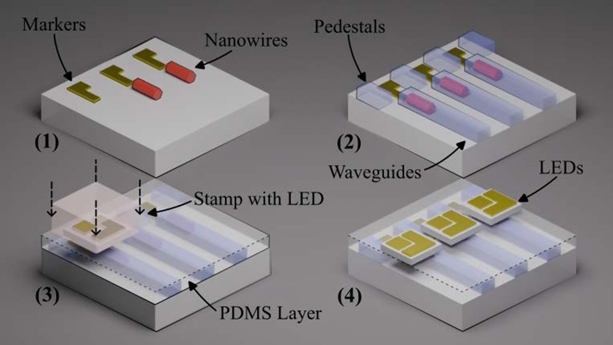
Schematic flow diagram showing the fabrication process of the nanowire system with transfer-printed micro-LED devices.
A research paper recently published in the journal Nanotechnology demonstrated the use of transfer-printed micro-light-emitting diode (LED) devices as single, integrated nanowire excitation sources for nanowire emitters.
Scalable Nanowire-based Systems
Over the last decade, research on nanowire emitters has made significant progress toward scalable nanowire photonic integrated circuitry (PIC), advancing from device-level investigations to system-level demonstrations. Currently, the focus of research is shifting towards addressing the scalability of advanced circuitry and inter-device variability.
The integration of nanowire technology into photonic circuitry is an active field of research, as the issues plaguing nanowire-based system development extend beyond device variability.
Heterogeneous and hybrid integration methods are suitable for assembling nanowire systems, as they provide flexibility in substrate and material selection and enable the transfer of both emerging and mature device technologies into photonic circuitry.
Yet, this integration technique incurs trade-offs in positioning accuracy, scalability, and time. Similarly, micro-tip-based systems face significant scalability challenges and require substantial time for device alignment and release/capture.
Micro-stamp-based methods, such as micro-transfer printing, can achieve serial integration speeds of over 1 device/minute at 500 nm integration accuracy. This integration method is commonly used for micro-/mini-LED and PIC assembly.
Scalable methods for nanowire detection and excitation are also crucial for transitioning this technology from laboratory demonstrations to real-world practical applications. Thus, exploring routes for individually addressable and in-parallel excitation of nanowire emitters is essential.
Previous studies have displayed the potential of micro-LED-on-complementary metal-oxide-semiconductor (CMOS) technology for optically exciting embedded nanowire circuitry. This scalable excitation approach allows independently addressable nanowire arrays with on/off-key modulation in the 100 MHz range by projecting micro-LED light patterns directly onto nanowire systems.
The Transfer-printed Micro-LED-based Approach
Based on advances in micro/mini-LED technology, which is now widely used in optogenetics and visible-light communications, researchers in this work presented a technique for scalable electro-optical on-chip addressing of semiconductor nanowire emitters using transfer-printed micro-LEDs.
In the proposed approach, the pumping elements were directly integrated on top of the nanowire circuitry, allowing small-signal modulation at tens of MHz rates and electro-optical addressing of nanowires.
This strategy also reduced the form factor of nanowire-based systems, opening the way to realizing programmable nanowire PICs without requiring nanowire post-processing or complex fabrication steps and bringing nanowire-based systems closer to chip-scale fabrication compatibility.
In this work, indium phosphide (InP) nanowire semiconductor nanoemitters with diameters of ~500 nm and lengths of 5–7 µm were used. They exhibited a high quantum efficiency of ~50% and supported room-temperature emission at a central wavelength of ~860 nm.
After growth, the nanowires were mechanically transferred onto host-circuitry substrates using bespoke soft microstamps, achieving sub-500 nm positioning accuracy through advanced alignment protocols. To enhance mode overlap with SU-8 6005 polymer waveguides, the nanowires were placed into waveguide cavities via a multi-step fabrication process.
In parallel, micro-LED membranes were fabricated from indium gallium nitride (InGaN) LED epitaxial structures grown on <111> silicon (Si) substrates, consisting of a 200 nm aluminum nitride (AlN) layer, a 950 nm aluminum-graded GaN buffer, an 800 nm n-type-GaN layer, a 100 nm multi-quantum well region, and a 140 nm p-type-GaN layer.
Optoelectronic characterization was performed using a 3-axis positioning stage with electrical probes driving the micro-LEDs, while free-space optics enabled imaging, alignment, and waveguide facet collection. After probe alignment, the setup was simplified, and further optimization was proposed via wire bonding and ceramic chip integration.
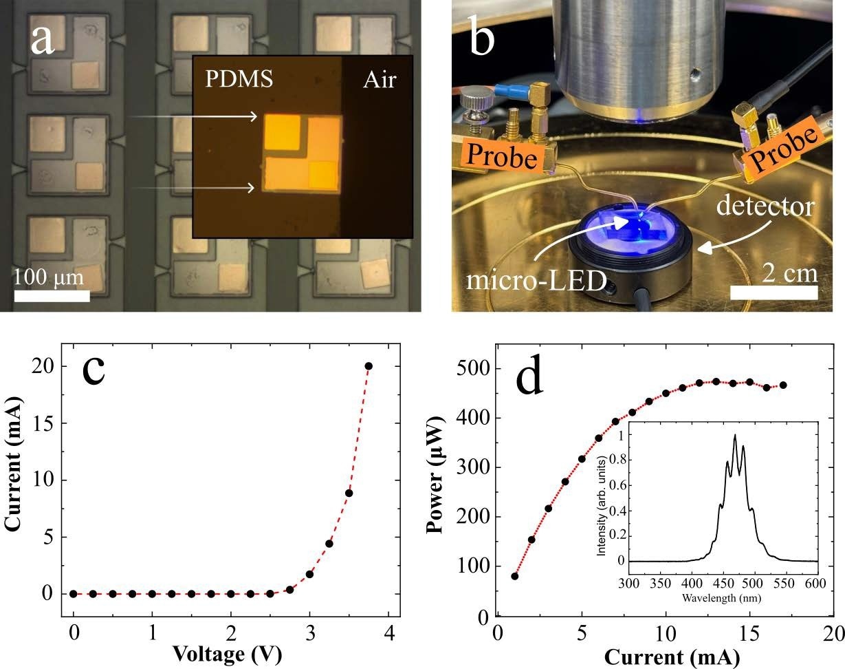
Micrograph showing suspended micro-LED array. Inset shows a micro- LED pixel heterogeneously integrated at the edge of a PDMS substrate. (b) Electrically probed micro-LED pixel on PDMS substrate, on a probing station. (c) I-V curve of the micro-LED-on-PDMS pixel. (d) Optical power measurement of the pixel with saturation region at around 10 mA. Inset shows the electro-luminescence spectrum of a representative micro-LED device.
Viability of the Approach
The findings demonstrated that individual waveguide-coupled nanowires exhibited small-signal modulation in the tens of MHz range at room temperature. Micro-LED integration with nanowire emitters on a chip enabled localized, scalable excitation without external optics.
The 470 nm emission from the micro-LEDs was absorbed by the nanowire device, which subsequently radiated near-infrared light at a central wavelength of approximately 860 nm as reported previously. Due to high divergence, the optical overlap between the LED emission area and the nanowire region was estimated to be below 1%.
With a measured power density of approximately 90 nW/µm², the optical power projected onto the nanowire was estimated at around 300 nW. This resulted in reduced quantum efficiency compared with conventional pulsed laser excitation due to lower pump power and the emission regime of the nanowire devices.
The authors also reported that the intensity measured at the waveguide facet from devices with nanowire emitters was approximately 2–3 times higher than that from bare waveguides, based on measurements from seven waveguide-integrated nanowire devices. To minimize unintended excitation of polymeric SU-8 waveguides, overlap with the integrated LED was reduced during alignment and printing by constraining geometry and coverage. Time-domain measurements over 20–120 MHz were filtered with a Savitzky–Golay filter to remove high-frequency noise.
To improve excitation fluence, the authors suggested introducing a meta-surface lens layer between the LEDs and the nanowire system to enhance light focusing and pumping efficiency. In conclusion, this study's findings demonstrated the feasibility of the proposed approach for realizing programmable high-density nanowire networks, although further optimization is required to transition the platform from a preliminary demonstration to practical applications.
Download your PDF copy by clicking here.
Disclaimer: The views expressed here are those of the author expressed in their private capacity and do not necessarily represent the views of AZoM.com Limited T/A AZoNetwork the owner and operator of this website. This disclaimer forms part of the Terms and conditions of use of this website.