The Semilab AFM-1000 is a state-of-the-art tabletop atomic force microscope designed to deliver high-resolution, sub-atomic, precise measurements with an extremely low noise level. It enables highly reproducible material characterization of a wide range of solid samples up to 65 x 65 mm (length x width).
Compact Design, Research-Grade Performance
Engineered as a compact tabletop AFM system with a small footprint, the AFM-1000 is well-suited for R&D environments where space and cost efficiency matter just as much as measurement quality. Its new design combines advanced instrumentation with a practical, user-friendly workflow tailored for academic and research laboratories in the field of materials science and nanotechnology.
Automation That Streamlines the Workflow
One of the AFM-1000’s key strengths is its high level of automation. The system can automatically perform a series of different measurements on a single sample, helping users improve throughput while reducing handling errors and operator-dependent variability. This makes it especially attractive for laboratories that need both precision and efficiency in their day-to-day work.
Precision Sample Handling and Alignment
The instrument is designed for easy and safe sample and cantilever handling, supported by a motorized sample stage and an integrated dual-focus camera system for laser alignment and tip-to-sample positioning. A manually adjustable laser path further increases flexibility during setup, while the choice of sample holder fixation by clamps or magnetic fixing helps accommodate different experimental needs.
Reliable Scanning Performance with Scan Area Customization Options
The AFM-1000 uses an AFM scanner with flexure-guided piezo positioners, enabling flat scanner movement and reliable scanning performance. In addition, customers can choose between the following two scan area customization options:
AFM-1000 Scan area customization options. Source: Semilab Semiconductor Physics Laboratory
| |
Option 1 |
Option 2 |
| Scan range |
50 x 50 µm |
100 x 100 µm |
| Z range |
5 µm |
10 µm |
| Stage range |
20 x 20 mm |
Built for Diverse Materials
The images show AFM-1000 measurement examples from a variety of materials, including silicon oxide calibration gratings, 6H-SiC-based calibration samples, aluminum nitride on sapphire, plasma-etched silicon, and even a soft polymer surface.
These examples underline the AFM-1000’s versatility in handling both hard and soft materials, making it a strong platform for researchers exploring nanoscale morphology, surface structure, and electrical characterization.
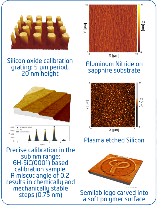
AFM measurement examples of various materials. Image Credit: Semilab Semiconductor Physics Laboratory
Why it Stands Out
For researchers, the AFM-1000 system offers a compelling balance of:
- Sub-atomic resolution
- Low-noise, reproducible measurements
- Automation-driven productivity
- Flexible scan and sample handling options
- A compact, tabletop form suited for R&D labs.
The Semilab AFM-1000 is a research-ready tool that combines precision, automation, and usability in one compact system. For scientists working at the intersection of materials science and nanotechnology, it offers a reliable route to deeper insights into nanoscale surface features.
For more information, you can visit the supplier webpage and read Semilab's latest AFM publications or request a quote.
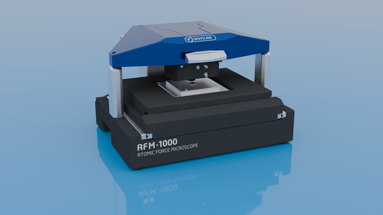
AFM-1000 system. Image Credit: Semilab Semiconductor Physics Laboratory
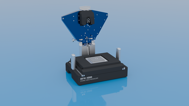
AFM-1000 system in open lid position. Image Credit: Semilab Semiconductor Physics Laboratory