The quantitative mechanical properties of small volumes of materials can be determined with the help of nanoindentation.
Nanoindentation: one technique for variable applications
A nanoindentation test provides accurate load-displacement curves for testing on both soft and hard surfaces. Nanoindentation is your key to unlocking quantitative mechanical properties of small volumes of materials. The technology is based on FischerCripps Laboratories’ successful nanoindentation system.
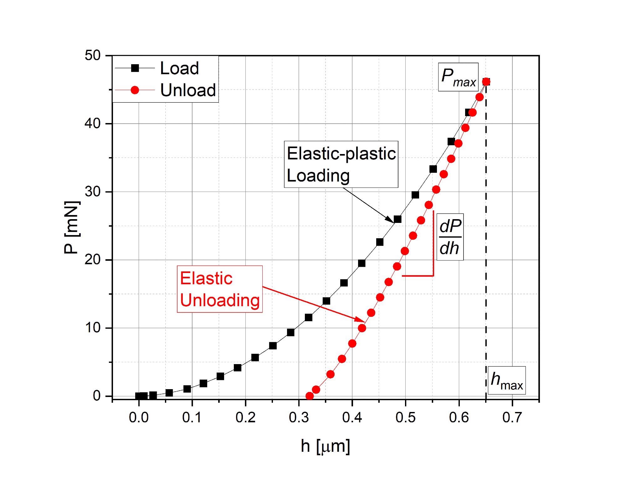
A load-displacement curve yield from nanoindentation test - Image Credit: Semilab Semiconductor Physics Laboratory
SEMILAB applies this metrology in two products from its nanoindenter family: the table-top IND-1000 and the advanced, stand-alone IND-1500 nanoindentation systems.
Nanoindentation technique is now a well-established method for determining elastic, plastic and visco-elastic properties of materials like: soft films, hard thin films, biological and composite materials, ceramics, plastics, semiconductors and multi-phase metals on a micron to nanometer scale. Nanoindentation testers are also applied for viscoelastic measurements of polymers and rough surfaces like those made by industrial processes such as thermal spray coatings, flexure testing of MEMS, and any application that needs mechanical measurement on the sub-micron scale.
What material properties can be measured with SEMILAB IND-1000 and IND-1500 Nanoindentation Systems?
- Elastic Modulus
- Hardness
- Yield Strength
- Storage and Loss Moduli
- Fracture Toughness
- Scratch and Wear properties - depending on the sample.
How does SEMILAB reach precise nanoscale measurements with IND product family?
SEMILAB Nanoindentation Systems are designed to convey a controlled load and deformation of the material under test.
The mechanical response of the material is quantified by using independent force and displacement sensors. The resolutions of the force and displacement sensors are extremely small (in the range of mN and μm with nm and nN resolution).
The high precision of the measurement enables recording of events on the micro-scale to the nanoscale. This allows interpreting and explaining macro-scale damage by events on the sub-micron scale, thereby enabling investigation and customization of the basic properties of the sample for specific applications.
SEMILAB Nanoindentation Systems use precise LVDT sensors for force and depth measurements. In this state-of-the-art package, AC amplification provides a μV noise floor. Exclusive circuitry ensures balancing of the signal to leverage the entire range of the analog-to-digital interface.
Notes: The use of LVDT measurement sensors for nanoindentation applications was pioneered by CSIRO in the late 1980s. From that time, with more experience, the technique has been well established, offering low-noise sub-nanometer resolution in a highly robust package.
Compared to competitor instruments that use a capacitance sensor, the IND system is virtually resistant to mechanical breakage due to overloading of the indenter shaft. This is because the indenter shaft directly passes through the sensor and can withstand unintentional deflection of several millimeters without any damage.
The force sensor is completely insulated from the load actuator and directly measures the force applied to the indenter, without any signal subtraction from support springs. The depth and force sensors are calibrated individually against international standards. Closed-loop feedback from the force sensor or the depth sensor can be selected. For high-speed data acquisition, users can even choose the open-loop operation mode.
Where Nanoindentation Meets Innovation
In 2024 Semilab engineers released a new design for the nanoindenter product family with more robust mechanics and a brand new software aiming academic, R&D and industrial users.
The IND-1500 instrument incorporates additional features of the IND-1000.
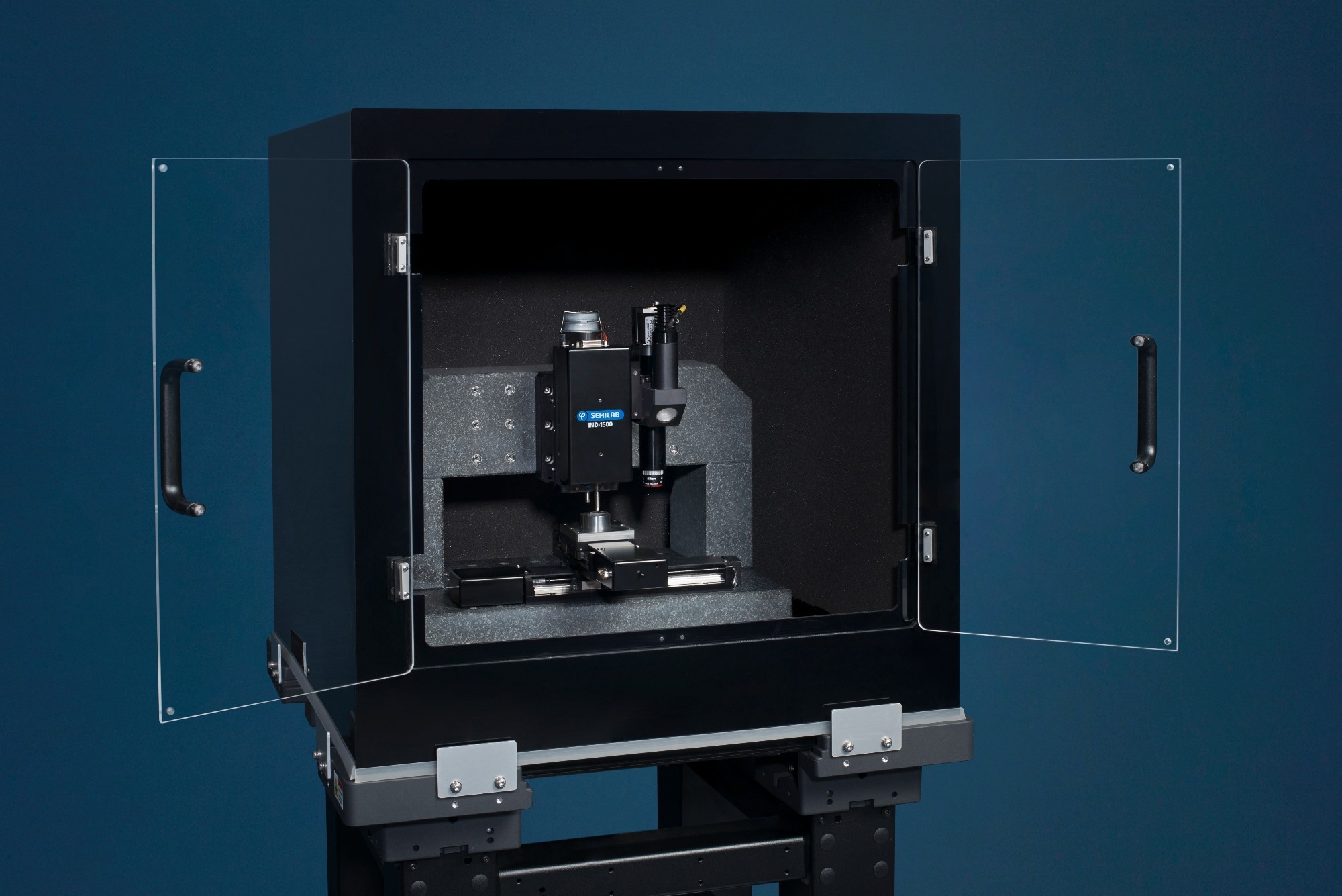
Closer look of IND-1500 Advanced Nanoindentation System - Image Credit: Semilab Semiconductor Physics Laboratory
Features of both Nanoindentation systems - IND-1000 & IND-1500
- High-resolution depth profile for Young’s modulus and hardness
- Highly linear response LVDT and sub-nanometer depth resolution
- PZT expansion element with excellent quality, without heat generation
- Dynamic and static measurement modes
- Closed-loop force/depth feedback
- Robust design withstands considerable overuse
- Low compliance load frame, mountings and acoustic enclosure
- Precise positioning of the sample ensured by video microscope and automated X-Y-Z-movement
- Real-time feedback control over application of depth- or load-independent force and displacement measurement
- Almost resistant to mechanical breakage when compared to competitor devices.
- Traceable calibration provided by SEMILAB
- Periodic calibration not needed
- Easy tip replacement
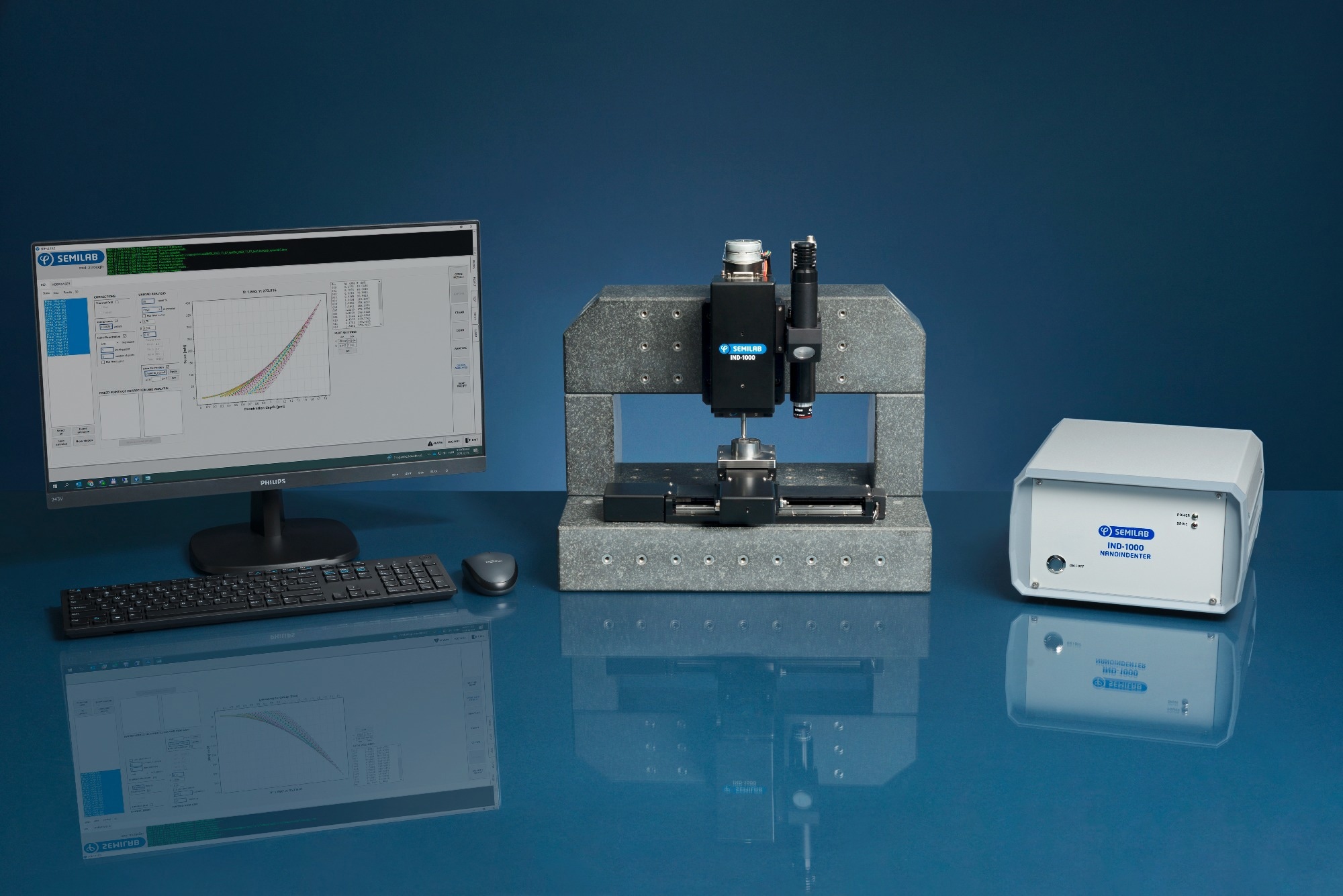
IND-1000 Nanoindentation Basic Tabletop System - Image Credit: Semilab Semiconductor Physics Laboratory
Optional Features of Nanoindentation Systems:
- Lateral force (Scratch Testing Module)
- Atomic force microscope: AFM on the same Z-axis
Additional benefits of the advanced IND-1500 system are:
- Improved vibration discharge
- Enhanced voice isolation
- Stand-alone, closable design.
SEMILAB Nanoindentation systems provide reliable performance for several years.
For more information, you can visit the supplier webpage or request a quote, and read the latest publications about Semilab nanoindentation systems’ various applications:
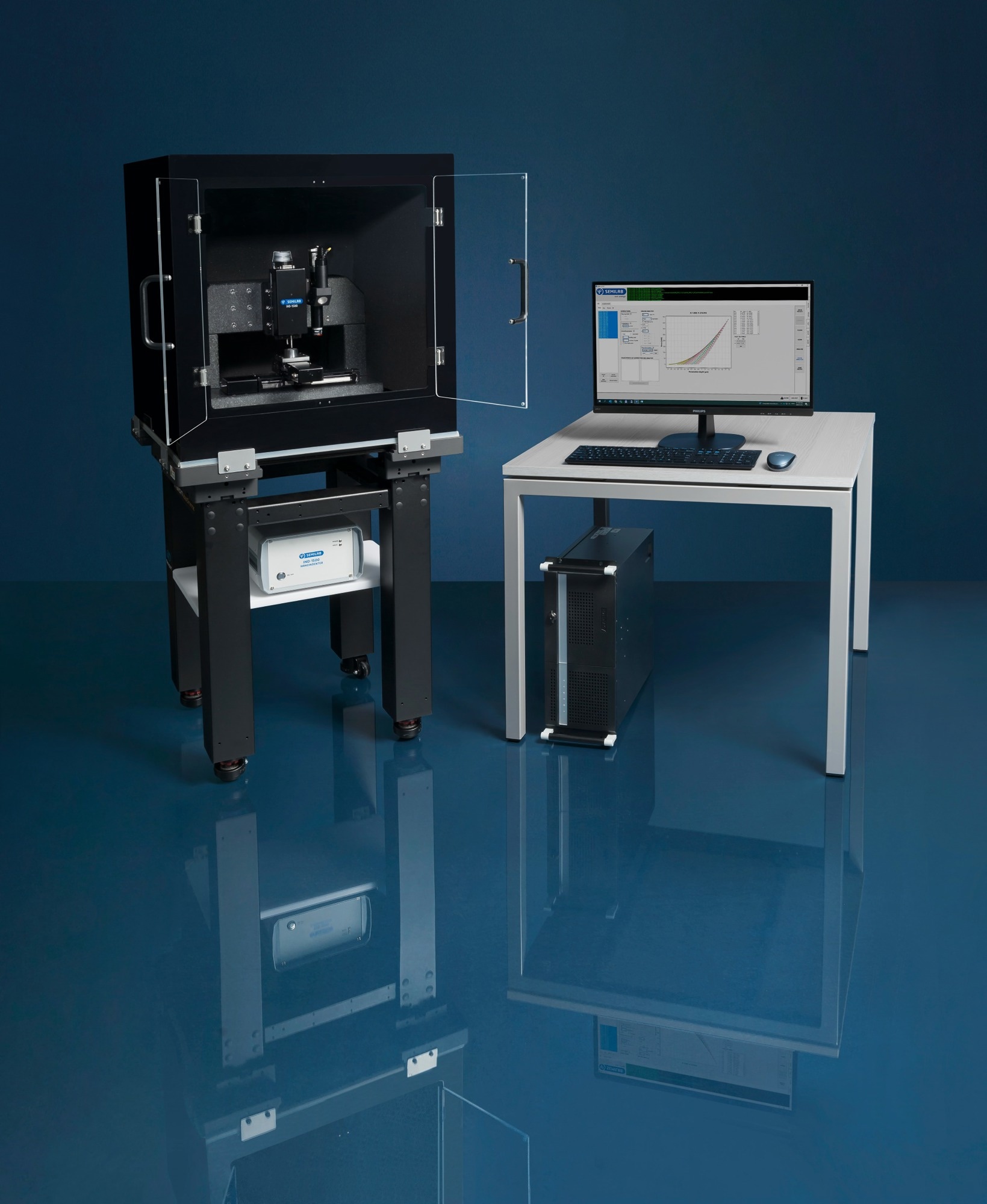
IND-1500 Advanced Nanoindentation System - Image Credit: Semilab Semiconductor Physics Laboratory