Nanowires are one-dimensional (1D) nanostructures that maintain their electrical conductivity even as their cross-section becomes smaller, unlike conventional electrical wires. Their electrical, optical, and magnetic properties are valuable in various applications, including computing, sensing, manufacturing, healthcare, data storage, and national security.1
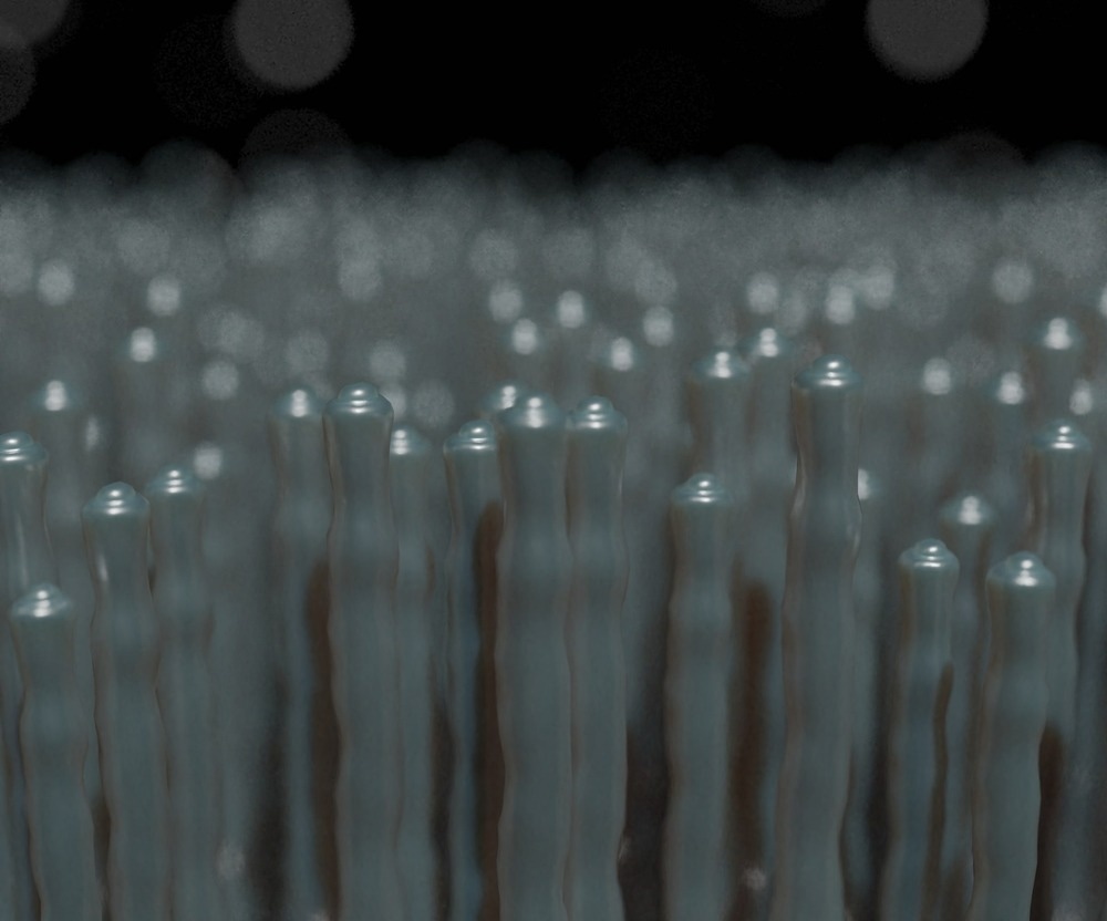
Image Credit: Love Employee/Shutterstock.com
The nanowire geometry can adapt to various materials, including metals, semiconductors, dielectrics, and polymers, resulting in nanodevices with unique functionality. The customizability of their composition, growth, crystal structure, and size positions nanowires as significant platforms for probing novel physical phenomena.2
Background and Structure of Nanowires
Nanowires are cylindrical nanostructures with diameters ranging from 10 to 100 nm and lengths that can be hundreds to thousands of times longer (1-10 μm).2 This high length-to-diameter ratio is responsible for their unique properties, including electrical conductivity and energy structure.1
Nanowires come in various types depending on their constituents. Conducting nanowires comprise metals such as nickel, platinum, gold, copper, and silver, while non-conducting nanowires are made from insulators like SiO2 and polymers. Additionally, molecular nanowires can be fabricated from organic or inorganic deoxyribonucleic acids.1
Elements from group III-V are most researched for nanowire systems. These include nanowires from single semiconductors (Si and Ge), composite semiconductors (InP, CdS, and GaAs), nitrides (GaN and Si3N4), carbides (SiC), functional oxides (ZnO and SnO2), ceramics (SiO2 and Al2O3), and composites (Si-Ge, SiC-SiO2).1,2
Nanowires with a core-shell structure are synthesized from two distinct materials. For example, silicon oxide nanowires comprise an amorphous oxide shell that prevents damage and contamination of the silicon core. Such hybrid nanostructures offer improved functionalities and novel properties.1
Quantum Mechanical Effects and Conductivity
The conductance of a traditional copper wire is governed by Ohm’s law, directly related to its cross-section and inversely to its length.2 However, since the width of nanowires is comparable to an electron’s wavelength, their conductance does not scale with cross-section. It is restricted by a definite value of 2e2/h (where e is electronic charge and h is Planck’s constant), known as the quantum of conductance.2
The natural confinement of electrons in a 1D conductance channel by the nanowire geometry and flexible material combinations allow their use in exploring various quantum transport phenomena, including ballistic flow of electrons, Coulomb blockade, quantum Hall effect, induced superconductivity, and spin transport.2
However, the conductivity of nanowires can be lower than their bulk counterparts. This is due to scattering resulting from collision between charge carriers, phonons, crystal defects, and impurities. Surface scattering, because of their large surface-to-volume ratio, limits the conduction even in flawless nanowires.2
Read More: How to Improve Nanowire Electrical Properties
Manufacturing Methods for Nanowires
Nanowires are generally manufactured using top-down and bottom-up methods.
In the top-down approach, bulk materials are reduced to nano size using lithography, etching, and electrophoresis techniques.1,2 This method produces nanowire arrays with enhanced control over arrangement and density, though it poses challenges like lithography limits, complex vertical formations, and non-customizable crystal structure and orientation.2
In the bottom-up method, nanowires are grown from constituent building blocks in an additive manner. Vapor-liquid-solid (VLS) growth is the most popular bottom-up technique due to its flexibility. It uses metal nanoparticles like gold to accelerate growth from a material supplied in the vapor phase.2
In the vapor-solid-solid (VSS) method, a variation of VLS, the catalyst remains solid throughout growth, yielding vertical nanowires. Selective-area epitaxy (SAE) is used for the non-catalytic growth of nanowires on masked substrates, where nanoholes function as nucleation sites. 2
Spontaneous nanowire growth is possible using evaporation and recrystallization processes, with surfactant molecules promoting growth in specific directions. Template-based methods are employed to grow nanowires using porous materials like zeolites, filling the cavities with colloidal nanoparticles via electrodeposition.1
Applications of Nanowires
The controllable electrical and optical properties of nanowires make them suitable for several applications. In electronics, carbon-based nanowires are widely used, such as graphite-diamond composite nanowires in electromechanical nano-switches and porous nanowires as efficient anodes in storage batteries.1
In photonics, semiconducting nanowires are used in several optical processes, including nonlinear optical mixing, room-temperature ultraviolet lasers, and subwavelength waveguiding. Nanowires also find applications in advanced microscopy and spectroscopy equipment.1
Research efforts are focused on reducing the size of optical components and improving device integration density, with polymer nanowires showing potential for compact photonic integrated circuits.1
Nanowires can reduce the size of existing transistors, overcoming the limitations of silicon electronics. For instance, nanowires do not generate heat during conduction, addressing a major challenge in increasing transistor density in integrated circuits.1
Metal nanowires, such as Ag and Cu, are promising for optoelectronic and microelectromechanical applications as advanced stretchable and transparent electrodes. These flexible transparent conductors offer low sheet resistance and high optical transmittance, making them ideal for optoelectronic devices like photovoltaic cells and touch panels.1
Nanowires are also well-established as powerful tools in healthcare. They can be located inside the human body as precise and efficient sensors to detect toxins and help eliminate them by loss-less transmission of ultraviolet rays. Additionally, nanowires integrated into blood vessels can stimulate the brain nerves, accelerating the identification of causes for neurological diseases like Parkinson's.1
Future Outlook
Nanowires have the potential to enhance functionality and ensure the integrity of next-generation devices at a low cost. Their processing and characterization according to target specifications can accelerate nanotechnology integration in various applications.1
A recent study in Materials highlighted the application of vertically aligned nanowires and quantum dots in light energy harvesting using solar cells. It reviewed various wet chemistry recipes for growing nanowires and surface functionalization with quantum dots. Promising photoconversion efficiencies were demonstrated with lead and zinc selenide quantum dots.3
Another recent article in Sensors presented a novel top-down synthesis approach for vertically stacked silicon nanowire (SiNWs) arrays without using wet oxidation, etching, and nanolithography. The integration of these SiNWs into body channel communication (BCC) circuits was also explored to develop an implantable pH sensing system for gastroesophageal reflux monitoring. The fabricated sensor validated the enhanced accuracy and efficiency of nanowires in implantable biosensors.4
Continuous research and development in nanowire manufacturing and materials will help overcome challenges related to limited conductivity and preferential growth direction, enhancing their practical applicability.
More from AZoNano: The Role of Nanotechnology in Endometriosis Treatment
References and Further Reading
1. Hsu, C.Y., et al. (2023). Nanowires Properties and Applications: A Review Study. South African Journal of Chemical Engineering. doi.org/10.1016/j.sajce.2023.08.006
2. Badawy, G., Erik. (2024). Electronic Transport and Quantum Phenomena in Nanowires. Chemical Reviews. doi.org/10.1021/acs.chemrev.3c00656
3. Prestopino, G., Orsini, A., Barettin, D., Arrabito, G., Pignataro, B., Medaglia, P. G. (2023). Vertically Aligned Nanowires and Quantum Dots: Promises and Results in Light Energy Harvesting. Materials. doi.org/10.3390/ma16124297
4. Kim, C., Han, S., Kim, T., Lee, S. (2024). Implantable pH Sensing System Using Vertically Stacked Silicon Nanowire Arrays and Body Channel Communication for Gastroesophageal Reflux Monitoring. Sensors. doi.org/10.3390/s2403086
Disclaimer: The views expressed here are those of the author expressed in their private capacity and do not necessarily represent the views of AZoM.com Limited T/A AZoNetwork the owner and operator of this website. This disclaimer forms part of the Terms and conditions of use of this website.