High-strain-rate loading occurs in many real-world scenarios, including vehicle collisions, drop and impact events, ballistic penetration, and high-speed machining processes. In these situations, materials typically show increased apparent strength, lower ductility, and failure behaviors that differ from those seen under slow loading conditions.
In-situ nanoindentation within a scanning electron microscope (SEM), performed at high strain rates, offers insights that are not accessible through quasi-static testing or post-mortem analysis. This approach makes it possible to observe the onset of plastic deformation, track how strain localizes, and directly visualize crack initiation and propagation as they happen.
This article introduces the approach to conducting in-situ high-strain-rate indentation in the SEM and includes a case study that quantifies the strain-rate sensitivity of tungsten at elevated temperatures.
Value of In-Situ High Strain Rate Testing
Rapid loading occurs during events including vehicle crashes, explosions, ballistic events, and abrupt mechanical shocks. In such instances, inertia effects become significant, and deformation may localize, often leading to phenomena such as adiabatic shear band formation or brittle fracture.
Applications requiring high-strain-rate testing cover a diverse range of sectors:
- Automotive and aerospace: Engineering structures capable of withstanding extreme loading rates, enhancing crashworthiness, and designing lightweight impact-resistant materials.
- Defense: Analyzing armor performance and penetration resistance.
- Microelectronics and MEMS: Comprehending rapid loading for drop impacts or thermal shocks.
- Nuclear materials research: Evaluating the behavior of irradiated material during accident scenarios.
High-strain-rate (HSR) testing describes the rapid deformation of a material over a very narrow time window. Although standard mechanical assessments are generally conducted at low strain rates, high-strain-rate conditions typically involve rates greater than ∼10 s-1, where deformation occurs on the order of microseconds to milliseconds.
Under these conditions, materials frequently behave differently, as limited time exists for dislocations to propagate, heat cannot dissipate efficiently, and stress cannot equilibrate throughout the material.
Consequently, materials frequently exhibit increased apparent strength, diminished ductility, and distinct deformation and failure modes under rapid loading.
Conducting high-strain-rate tests in situ is critical, as it enables direct observation of material deformation and failure during rapid loading, instead of depending on post-test evaluation or indirect measurements.
By integrating methods like SEM or high-speed imaging, in-situ testing allows scientists to observe where plastic deformation begins, how strain localizes, and how cracks nucleate and propagate in real time. This offers a fundamental understanding of deformation mechanisms that cannot be captured through traditional assessments.
The Hysitron PI 89 and PI Envision SEM PicoIndenters can perform high-strain-rate mechanical assessments using high-stiffness transducers (500 mN and 3.5 N) equipped with Direct Drive (DD) piezo flexure actuation.
The PI 89 can reach maximum strain rates surpassing 1000 s-1, whereas the PI Envision supports strain rates exceeding 100 s-1, enabling researchers to investigate material behavior across a diverse range of dynamic deformation regimes.
A key advantage of both systems is that they do not require any additional or specialized hardware beyond what is already used for quasi-static testing. High-strain-rate experiments can therefore be carried out not only at room temperature but also at cryogenic and elevated temperatures.
Case Study: Strain-Rate Sensitivity from Ambient Temperature to 250 °C
Methods
Every assessment was conducted with a Hysitron PI 89 SEM PicoIndenter featuring a Direct Drive (DD) piezo flexure (maximum displacement of 30 μm) and an xR High Load transducer (maximum force of 3.5 N).
Indentations were conducted at a constant, defined strain rate in displacement control to a maximum depth of 1000 nm. Here, the strain rate,  , is calculated as the ratio of the displacement rate to the displacement.2 This loading condition requires displacement to follow an exponential function of time.
The PI 89 can maintain the same strain rates, as high as approximately 1000 s-1, across a broad thermal range.
In this study, fused quartz, a nanoindentation standard specimen, was evaluated with a diamond Berkovich probe at ambient temperature using strain rates of 1, 10, 100, and 500 s-1.
Polycrystalline tungsten with an approximately 30 μm grain size was assessed with a cubic boron nitride (cBN) Berkovich probe at 250 °C using strain rates of 1, 10, 100, and 1000 s-1.
Using SiC metallographic paper, the tungsten sample was ground down to 1200 grit, followed by polishing with diamond suspension (3 μm, 1 μm) and finishing with 0.03 μm colloidal silica.
Due to the high speeds at which indentation is carried out, conventional nanoDynamic (oscillatory) testing (which is used to continuously measure contact depth, hc) is not feasible. Instead, certain assumptions are required to determine how mechanical properties vary with depth under high-speed conditions.
A common approach is to assume that the ratio of contact depth to total displacement remains constant throughout the indentation (i.e., it is treated as a constant, hc/h = “constant”).2
This assumption, combined with the calibrated area function from the standard Oliver–Pharr method, enables the calculation of hardness over the course of the test.1
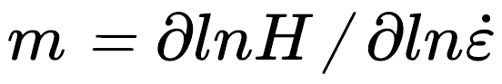 , describes the change in yield strength (or hardness) as the applied strain rate changes.3
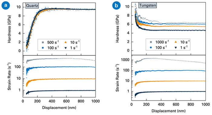
Figure 1. (a) Hardness (above) and strain-rate (below) profiles of fused quartz at room temperature, showing little variation in hardness with applied strain rate. (b) Hardness (above) and strain-rate (below) profiles of tungsten at 250 °C, showing substantial hardness changes with applied strain rate. Image Credit: Bruker Nano Surfaces and Metrology
Results
Figure 1a displays the strain rate and hardness profiles for fused quartz at ambient temperature.
As anticipated, the hardness exhibits little variation between strain rates because fused quartz deformation is strain-rate insensitive.
Figure 1b illustrates the strain rate and hardness profiles on the tungsten specimen indented at 250 °C. In this case, the measured hardness demonstrates significant variation as the strain rate increases.
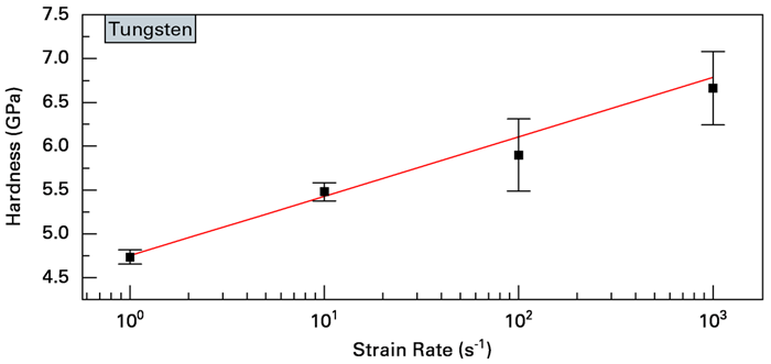
Figure 2. Average hardness as a function of applied strain rate for tungsten at 250 °C. The slope of the line is the strain rate sensitivity and is approximately 0.05. Image Credit: Bruker Nano Surfaces and Metrology
To determine the material’s strain rate sensitivity, hardness versus strain rate can be plotted on a log-log plot, as illustrated in Figure 2. The slope of the fit, m, in Figure 2 represents the strain-rate sensitivity and is roughly equal to 0.05 at 250 °C. This change correlates well with earlier measurements conducted on single-crystal tungsten.4
The PI 89 and PI Envision Facilitate In-Situ High-Strain-Rate Indentation in the SEM
The Hysitron PI 89 and PI Envision SEM PicoIndenters enable controlled, quantitative in-situ high-strain-rate nanoindentation assessment in the SEM from ambient temperature to elevated temperatures without requiring specialized add-ons.
In this case study, a strain rate–insensitive reference demonstrated stable hardness across the tested range, while tungsten at 250 °C showed a clear positive rate dependence with a strain-rate sensitivity of approximately 0.05.
Such high-strain-rate testing capabilities, particularly the ability to carry out experiments at high temperatures, are important for industries dealing with rapid loading, including automotive, aerospace, defense, microelectronics, and nuclear sectors.
Acknowledgments
Based on materials originally authored by Kevin Schmalbach, Sanjit Bhowmick, and Eric Hintsala, all of Bruker.
References and Further Reading:
- Oliver, W.C. and Pharr, G.M. (1992). An improved technique for determining hardness and elastic modulus using load and displacement sensing indentation experiments. Journal of Materials Research, 7(6), pp.1564–1583. DOI: 10.1557/jmr.1992.1564. https://link.springer.com/article/10.1557/JMR.1992.1564.
- Hackett, B.L., et al. (2023). Advances in the measurement of hardness at high strain rates by nanoindentation. Journal of Materials Research, 38(5), pp.1163–1177. DOI: 10.1557/s43578-023-00921-1. https://link.springer.com/article/10.1557/s43578-023-00921-1.
- Maier, V., et al. (2014). Microstructure-dependent deformation behaviour of bcc-metals – indentation size effect and strain rate sensitivity. The Philosophical Magazine A Journal of Theoretical Experimental and Applied Physics, 95(16-18), pp.1766–1779. DOI: 10.1080/14786435.2014.982741. https://www.tandfonline.com/doi/abs/10.1080/14786435.2014.982741.
- Kappacher, J., et al. (2020). Thermally activated deformation mechanisms and solid solution softening in W-Re alloys investigated via high temperature nanoindentation. Materials & Design, 189, p.108499. DOI: 10.1016/j.matdes.2020.108499. https://www.sciencedirect.com/science/article/pii/S0264127520300320.

This information has been sourced, reviewed and adapted from materials provided by Bruker Nano Surfaces and Metrology.
For more information on this source, please visit Bruker Nano Surfaces and Metrology.