Pressurex® film from Sensor Products Inc. is a quick, accurate and economical way to detect and correct pressure variations which can result in flaws (defects) in the wafer bonding process. When placed between contacting surfaces, it instantaneously and permanently changes color directly proportional to the actual pressure applied. With Pressurex®, variations in pressure that lead to imperfections (or irregularities) in the bonding process can be accurately detected and corrected -- improving yield, decreasing scrap, and boosting productivity.
In wafer bonding, two flat substrates are permanently joined together by applying carefully calculated pressure, temperature, and voltage. Of the three parameters, pressure is often the most difficult to precisely ascertain and control. Traditional methods assume perfectly flat pressure plates. However, in nearly all real environments pressure plates are not ideal due to manufacturing or installation variability and degradation over time from wear. The result is difficult to detect pressure variations across the surface that can lead to un-bonded wafer areas, cracked wafers, and premature wear of the pressure plates.
Pressurex® systematically measures pressure across the entire pressure plate. When placed between contacting surfaces of the wafer bonding fixture, the film instantaneously and permanently changes color directly proportional to the actual pressure applied. Precise pressure magnitude is easily determined by comparing color variation results to a color correlation chart (conceptually similar to interpreting Litmus paper). Additional pressure analysis of the film is available which assimilates the pressure distribution into 2-D and 3-D pseudo color images, histograms and line scans among other features.
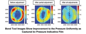
Micralyne Inc. uses Pressurex® to adjust the compression exerted by their bonding tools. Early testing of bonding results analyzed with the film reveals a donut shaped high pressure ring with relatively little pressure applied to the center ((left)). After a series of adjustments the final result is a more uniform distribution of pressure.
Wafer-to-wafer bonding has become an enabling semiconductor technology in industries such as 3D packaging, MEMS, MOEMS, and SOI. Pressurex® is being used across a wide range of bonding technologies, including metal eutectic, anodic, fusion, metal diffusion, glass frit, and polymer adhesive bonding
The “snapshot” imaging results of Pressurex® can be used as a control to compare processes and tools, making it ideal for six-sigma and other closely monitored high performance manufacturing operations.
Pressurex® measures pressures from 2 - 43,200 PSI (0.14 - 3,000 kg/cm2). For a free sample in your desired range, contact Sensor Products Inc. at 1.973.884.1755 (USA), email [email protected] or visit their website at www.sensorprod.com/sample where you can view their entire line of products and applications.
Headquartered in New Jersey and established in 1990, Sensor Products Inc. is a world leader in the manufacture and distribution of tactile pressure sensing solutions. Their customized and off-the-shelf products are installed within all of the Fortune 500 industrial companies as well as thousands of smaller manufacturing firms. Their sensors are used in applications as diverse as tire testing to semiconductor manufacturing and from R&D labs to space missions. Additionally, Sensor Products provides in-house and on-site stress and pressure mapping analysis, as well as a variety of regional technical seminars.