Whether inspecting semiconductor wafers, measuring optical components, or imaging biological samples, the quality of the data depends on maintaining perfect focus. Modern microscopes and surface metrology systems often work at high magnifications where the depth of focus can be only a few micrometers –or even less. A slight change in sample height, surface topography, thermal drift, or vibration can quickly move the area of interest out of focus, degrading image quality and measurement accuracy.
 PI’s nanofocusing stage options–voice coil (left) for longer travel, piezo (right) for minimum size and fastest response. Image Credit: PI (Physik Instrumente) L.P.
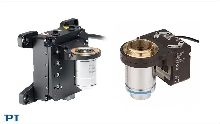
Options – Piezo and Voice Coil
Fast nano-precision focusing systems such as PI’s piezo-driven P-725 and voice-coil-driven V-308 solve this challenge by continuously adjusting the objective lens or sample position with nanometer-level resolution and millisecond response times. In optical profilometry and 3D surface metrology, rapid focus scanning enables accurate reconstruction of complex surface features, while in automated microscopy it allows large areas or multiple samples to be inspected without sacrificing image sharpness.
Semiconductor Inspection / Metrology
The combination of high speed and nanometer precision is especially important in semiconductor inspection, where millions of features must be measured quickly and accurately. By minimizing focus errors and reducing settling times, precision focusing systems increase throughput, improve repeatability, and enable reliable detection of increasingly smaller defects and structures. As imaging resolutions continue to improve and production demands increase, fast nanopositioning focus systems have become a critical enabling technology for next-generation metrology and microscopy equipment.
Achieving nanometer precision in milliseconds, not only requires precision mechanics and sensors, but also advanced electronics and control algorithms. PI provides benchtop and OEM digital motion controllers with advanced linearization and optimization for both scanning and fast step & settle applications.
Industries Served and Applications
Semiconductor inspection, Metrology, DNA Sequencing, Microscopy, Photonics, Laser Processing.