Imprint lithography is a cost efficient technology to create an optimal surface texture on solar cells, cover glasses and polymeric films. For silicon solar cells anti-reflection surface texture not only decreases reflection, but also increases the forward scattering of the incident light. For thin film cells a large scattering angle increases the optical path length of the photon within the cell. A reflection layer at the backside of the cells enables light trapping within ultra-thin film PV cells. Micro-optical elements enable the integration of beam shaping elements with a very small form factor.
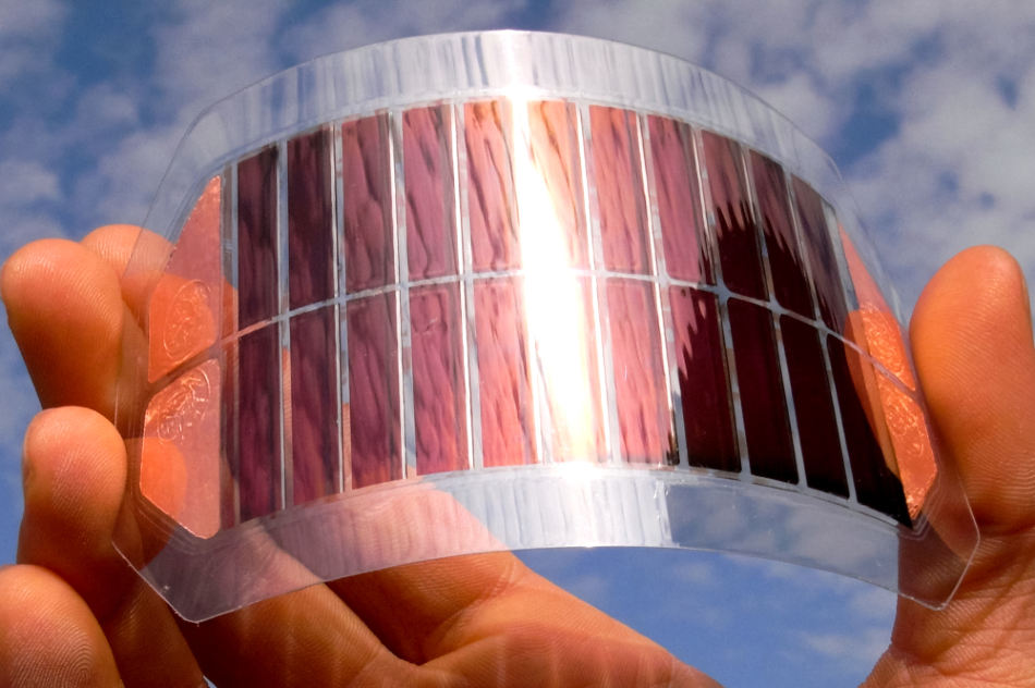
Image Credit: Shutterstock/LuYago
Light Trapping
Imprint lithography allows to create optimal surface texture on large areas directly on the cover glass as well as on the wafer level. The imprinted film can be either used directly or as an etch mask. For crystalline silicon cells the texture is optimized in such a way to minimize reflection and optimize forward scattering. For thin film cells the texture is optimized for light trapping within the cell.
Light trapping is an important concept which allows to minimize material consumption and absorber layer thickness. The combination of frontside texture, which deflects the incident photons into the cell, and backside texture, which reflects the photons back into the cell enable effective total reflection within ultra-thin film solar cells. Even complex structures like photonic crystals and quasi-periodic photonic crystals can be created by NIL on a large scale. Nanopillars enable new thin film cell architectures for "electrically thin, optically thick" cells.
.jpg)
Figure 1. SEM close up of 350 nm photonic crystal. Master provided by NILT.
.jpg)
Figure 2. Nanopillars created by Nanoimprint Lithography (NIL).
Courtesy of CIHR-NRC Convergent Research Framework 2004
Dirt Repellent Texture
Debris and dirt on the PV module causes rapid deterioration of the real performance. Dirt repellent films on the cover glass enable a self cleaning effect thereby enhancing the real module performance significantly over the whole module lifetime.
.jpg)
Figure 3. Dirt repellent functional layers reduce accumulation of debris and enable a self cleaning effect on the PV glass.
Micro Optics
UV Imprinting provides an easy and cost efficient manufacturing process for micro-optical elements. UV imprinting enables the replication of any kind of optical features: spherical and a-spherical lenses, diffractive optical elements and functional optical films. Microlenses focus and concentrate the incident light directly on the photovoltaic cell. With microlenses it is possible to use multiple micro-PV cells instead of large CPV cells. The form factor of CPV modules using micro-optics is significantly smaller enabling ultra-thin and ultra-light CPV modules.
.jpg)
Figure 4. Microlenses couple the light into a waveguide, which allows superior form factor and reduced costs.
Photo courtesy of Jason Karp, UC San Diego
.jpg)
Figure 5. Aspherical microlenses
.jpg)
Figure 6. Diffractive optical elements
Process Flows
.jpg)
Figure 7. Process flow for Hot Embossing
.jpg)
Figure 8. Process flow for UV Nanoimprint Lithography
.jpg)
Figure 9. Process flow for Soft Stamp Fabrication

This information has been sourced, reviewed and adapted from materials provided by EV Group.
For more information on this source, please visit EV Group.