A time correlated single photon counting module can be easily attached to the alpha300 or alpha500 confocal microscope, thanks to the modular design of the WITec microscope series. Hence, several types of time-resolved and spatial measurements are possible such as fluorescence lifetime imaging or electro- and photoluminescence decay imaging. This article covers spatially resolved electroluminescence (EL) studies of a blue, light-emitting diode (LED).
Spatially and Time-Resolved Electro- and Photoluminescence
Standard characterization techniques for optoelectronic devices include spatially resolved electro- and photoluminescence measurements. These are essential tools during lifetime and failure studies. Both methods, µPL and µEL, determine the luminescence decay spectrally and spatially resolve the same through a microscope objective. However, in µEL a bias voltage is utilized and in µPL a laser is utilized to excite the luminescence.
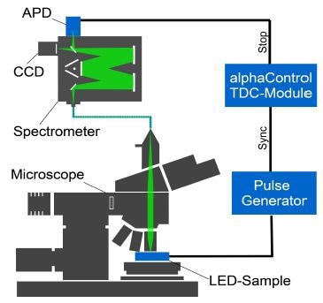
Figure 1. Micro electroluminescence setup based on an alpha300 for time resolved luminescence measurements
In case of the µEL, it is possible to drive the device under different electrical conditions, while in µPL the power and excitation wavelength of the exciting laser can be changed.
System Setup
Figure 1 illustrates the µEL measurement setup based on an alpha300 microscope fitted with a time-correlated single photon counting (TCSPC) module for time-resolved measurements.
A short electrical pulse for triggering LED emission is generated using a pulse generator (HP 8082A). A high numerical aperture (NA) objective (6ox, NA= 0.7) collects the light illuminated from the LED. The objective forms an image, which is projected onto a multimode optical fiber (25µm diameter, NA=0.12). The fiber then picks up the light from a single point (0.42µm diameter, nearly diffraction limited) of the LED and guides it to a spectrometer fitted with a single photon counting detector and a BI-CCD camera. Sample was scanned using a piezo electric span stage with respect to the detection fiber.
Full luminescence spectra was acquired at every sample position while the single photon counting APD was employed to measure the time resolved luminescence decay at selected spectral positions. Owing to this reason, the NIM output of the APD (MPD PDM1CTC) was linked to a time-to-digital converter (TDC) extension board in the alpha control microscope controller. The time between the excitation pulse and the arrival of a luminescence photon at the APD is measured by the extension board. A histogram of these arrival times is used to plot the luminescence decay curve.
Sample Used
A commercial blue/green LED was studied with this set-up. These LEDs are normally based on InGaN III-V-compound semiconductors. A variation in the ratio between Indium (In) and Gallium (Ga) causes the semiconductor band gap to change from 3.49 eV (GaN) to 0.65 eV (InN), covering the complete visible spectrum.
Multi Quantum well structures are components of LEDs and semiconductor lasers. Producing homogeneous InGaN layers is a big challenge in thin-film epitaxy. Indium tends to form small clusters within the InGaN matrix due to phase separation. The varying Indium concentration results in a spatially 600 varying band gap, which changes the local emission spectrum of the diode. Figure 2 illustrates a microscope image of a blue LED at low magnification.
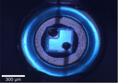
Figure 2. Video image of blue InGaN LED.
Micro-Electroluminescence Measurement
The variation of the emission spectra can be quantified with a µEL measurement at higher resolution. Inhomogenous broadening is seen although each spectrum is a local spectrum from a small region of the sample. Hence, a Gaussian curve fit is a good approximation for the emission spectra. Figure 3 depicts the Gaussian curve fit for the emission spectra.
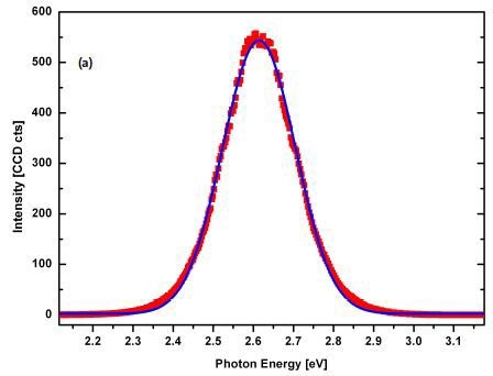
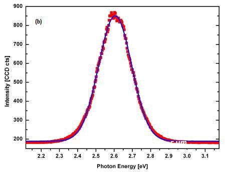
Figure 3. Gaussian curve fit of the emission spectra. a): Average spectrum of image scan (Fig. 4) together with Gaussian fit curve; b): Single spectrum of image scan (Fig. 4) together with Gaussian fit curve.
The region between the two bond pads is shown in Figures 4a-c. The µEL image contains 270 x 270 = 72900 spectra with a 12ms integration time for each spectrum. The intensity, spectral width, and spectral position are obtained by fitting a Gaussian curve to the spectra. The intensity is shown in Figure 4a, the spectral center in Figure 4b, and the spectral width in Figure 4c.
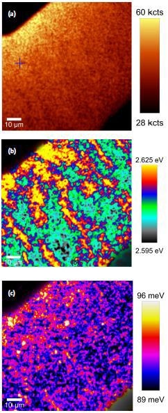
Figure 4. μEL measurement at the region between the two bond pads on the LED.
Time-Resolved Emission Spectroscopy (total area)
The temporal decay of the emission at different wavelengths can be measured with a TDC extension board. The diode was excited with a short electrical pulse of 2ns duration at a repetition rate of 2MHz for this experiment. Three different time spectra at photon emission energies of 2.756eV, 2.611eV and 2.480eV, respectively are shown in Figure 5. These time spectra are far from single exponential because of the inhomogeneous distribution of Gallium and Indium.
For obtaining an average relaxation time, the full width at half maximum (FWHM) of the emission time spectra was studied. Figure 6 shows the relaxation time against photon emission energy. The relaxation time falls from 15ns to 2ns with increasing energy. At peak of the emission spectrum, the strongest decrease of the relaxation time is observed.
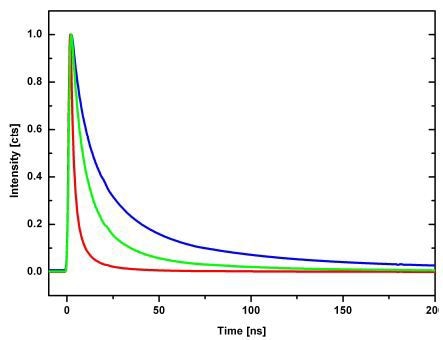
Figure 5. Time spectra at 450nm <=> 2.756 eV (red), 475nm <=> 2.611 eV (green) and 500nm <=> 2.480 eV (blue).
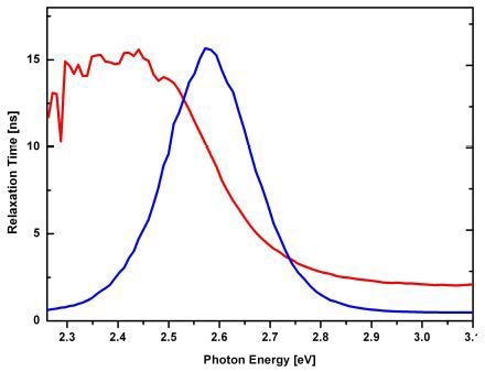
Figure 6. Relaxation time (red) and intensity (blue) vs. photon energy.
Time-Resolved Emission Spectroscopy (local)
The relaxation time also varies locally and is not just a function of photon energy. It is possible to acquire spatially-resolved time spectra at fixed wavelengths instead of emission spectra using the same set-up. From these time spectra, a map of local relaxation times can be calculated. Figure 7 illustrates the spatially varying relaxation times at photon emission energies of 2.756eV, 2.611eV and 2.480eV respectively.
The reason for this variation is multi-layered. A potential landscape for electrons and holes is created by the variation of the indium concentration. The carrier diffusion is restricted at flat and large potential valleys. This also impacts the local relaxation time since surrounding carriers will flow to this valley. Electrons and holes are trapped in the so-called quantum dots. This localization process increases the lifetime of the direct electron-hole-recombination dramatically.
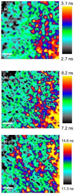
Figure 7. Spatially varying relaxation times at photon emission -500 0 500 1000 1500 2000 2500 energies of 2.756 eV (450 nm), 2.611 eV (475 nm) and 2.480 eV (500 nm) respectively.(a): Relaxation time at 45onm;(b): Relaxation time at 475nm; (c): Relaxation time at 500nm.
Signal Propagation Through the Device
The temporal decay of the emission does not just vary in space but also at its starting point. The luminescence emission is delayed for areas that have a larger distance to the bond pad of the back-side contact.
Conclusion
Thus, blue LEDs can be effectively studied using standard characterization techniques like spatially and time-resolved electro- and photoluminescence.

This information has been sourced, reviewed and adapted from materials provided by WITec GmbH.
For more information on this source, please visit WITec GmbH.