Image Credit: Macro photo/Shutterstock.com
After nearly three decades of development, a new generation of ASML's integrated circuit fabrication tools is now available to semiconductor chip manufacturers. The new production line employs a state-of-the-art extreme ultraviolet (EUV) lithography process using light with a wavelength of 13.5 nm to bring the silicon building blocks of the future innovative CPU chips down few nanometers in size.
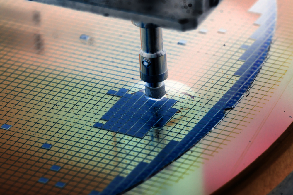
Up until now, chipmakers have employed a photolithographic process that uses ultraviolet (UV) light to project complex patterns onto silicon wafers coated with a photosensitive polymer (called photoresist). The process is analogous to the development of the old paper photographs; the illuminated patterns are developed, etched, or coated with metal to isolate or conduct structures within one layer of the integrated circuit structure. This process can be repeated hundreds of times, layer by layer, until the complex interconnected network of transistors forming an integrated circuit, such as a microprocessor, is complete.
Densely Packed Integrated Circuits Designs
The ever-growing demand for computing power and data storage capacity, together with the need to reduce costs and power consumption, drive computer chip manufacturers in their pursuit of more advanced and efficient integrated circuit designs.
Over the past five decades, the development of newer generations of computer chips follows a simple rule known as Moore’s law, which states that the number of elements in the densely packed integrated circuits doubles approximately every two years.
The Spatial Resolution Barrier
A significant limitation for the continuous shrinking of the transistor size in modern silicon chips comes from optics laws. At the end of the 19th century, the German physicist Ernst Abbe found that the resolution of an optical microscope (the smallest resolvable distance between two features of the sample) is proportional to the wavelength (λ) of the light used for the sample illumination and inversely proportional to the refractive index of the medium between the microscope lens and the sample.
The same principle is valid for any light-based projection system, including the photolithographic semiconductor fabrication tools. This is why the wavelength of the light used in the photolithography process plays a crucial role.
Shorter Wavelengths for Smaller Transistors
As a result, scientists and engineers have been looking for light sources with ever-shorter wavelengths to produce smaller features within the semiconductor chips. Beginning with UV mercury-vapor lamps when the transistor size dropped below 1 µm in the middle of the 1970s, they moved to powerful argon fluoride (ArF) excimer lasers producing a deep UV (DUV) light with λ=193 nm and later on λ=157 nm.
These developments allowed chip manufacturers to dramatically increase the transistor density in the semiconductor chips over the last couple of decades by shrinking the chip's logical element features down to 130 nm, then 65 nm, and finally under 20 nm. This helped produce faster and more efficient integrated circuits at a reduced cost.
Historically, the metric in nanometers referred to the smallest actual size of the transistor gate that a given lithographic process could produce. These numbers have become nominal and indicate the different manufacturing processes that chipmakers are using and are known as technological nodes.
An ever-growing volume of mass-produced integrated circuits is currently moving beyond the 10 nm boundary towards the 7 nm technological node and below.
Numerous applications such as mobile computing with 5G connectivity, artificial intelligence, autonomous driving, and high-performance computing would benefit significantly from the increased performance and energy efficiency that the next generation of innovative CPU chips can offer.
Next-Generation Lithographic Systems for the Semiconductor Industry
To keep up with the demand, three of the key semiconductor manufacturers, TSMC (Taiwan Semiconductor Manufacturing Company), Intel, and Samsung, have adopted the TWINSCAN NXE:3400C EUV lithography scanner, the latest and most advanced of the ASML's semiconductor fabrication tools and the only commercially available EUV lithographic system.
With more than 100,000 components, the TWINSCAN NXE:3400C is one of the most complex machines ever built. Its EUV light source is pumped by the most powerful serially produced laser system. The machine weighs 180 tons and consumes more than 1 MW electrical power in total, and costs $120 million.
EUV Light Source for the Industry
At the core of the machine is the EUV optical system developed by Zeiss SMT (Carl Zeiss Semiconductor Manufacturing Technology, based in Oberkochen, Germany, and ASML's long-term partner). EUV radiation denotes soft X-rays with wavelengths between 124 nm and 10 nm. Stars produce EUV light in the superheated plasma of their coronas.
Zeiss scientists and engineers developed a unique light source, aptly named Starlith®, that generates laser-pulsed-plasma (LPP), which emits EUV light with λ=13.5 nm. The light source is pumped by a 40 kW CO2 laser pulsed 50,000 times a second (manufactured by the German company Trumpf, based in Ditzingen). Each laser pulse instantly evaporates a tiny droplet (10-20 µm in diameter) of molten tin that is turned into superheated EUV-emitting plasma.
EUV Lithography Enables the Fabrication of Innovative CPU Chips
The EUV optics within the NXE:3400C is designed from scratch and is entirely mirror-based (as there are no materials transparent to EUV). The tin plasma's plasma radiation is collected with a huge aspherical mirror with an average reflectivity at 13.5 nm of around 40%. A set of ultraprecise mirrors further shapes the EUV beam from the collector mirror. It illuminates the reticle (or the photomask) that contains the complex patterns to be transferred onto the silicon wafer surface. From the reticle, the patterned EUV beam is projected onto the wafer surface by the second set of ultra-flat mirrors, with a 250 W of power delivered to the wafer surface, and a throughput of 170 wafers exposed per hour with a spatial resolution of only 13 nm.
The improved spatial resolution of the EUV lithographic process offers a significant reduction in the chip fabrication process's complexity, together with increased design flexibility, shorter fabrication time, lower cost, and superior electrical circuit properties of the final product.
Owing to ASML's NXE:3400C EUV lithography scanners, TSMC is already rolling out its commercial chips manufactured on the company's 5nm process node, including Apple's latest A14 processor used in the flagship iPhone 12. Other chip manufacturers will follow with innovative CPU chips, advanced memory, and fast and energy-efficient integrated circuits for 5G connectivity.
What Comes After EUV?
The engineers at ASML and Zeiss SMT are already anticipating the next developments that might allow chip manufacturers to pack more logical elements and memory into their semiconductor devices.
To answer the demand for even higher lithographic resolution, ASML and Zeiss SMT are developing the high numerical aperture EUV (or high-NA EUV) scanners (announced as NXE Next). The numerical aperture of an optical system is a measure of how much light the optics can deliver to the sample surface and is one factor that determines the system's spatial resolution. The current EUV optical system has reached an NA of 0.33. The next generation of EUV scanners will have an NA of 0.55, enabling a spatial resolution of less than 8 nm.
References and Further Reading
ASML (2020) TWINSCAN NXE:3400C. [Online] www.asml.com Available at: https://www.asml.com/en/products/euv-lithography-systems/twinscan-nxe3400c (Accessed on 27 October 2020).
A. Shilov (2020) ASML Ramps Up EUV Scanners Production: 35 in 2020, Up to 50 in 2021. [Online] www.anandtech.com Available at: https://www.anandtech.com/show/15428/asml-ramps-up-euv-scanners-production-35-in-2020-45-50-in-2021 (Accessed on 27 October 2020).
M. Lapedus (2020) EUV’s Uncertain Future At 3nm And Below. [Online] www.semiengineering.com Available at: https://semiengineering.com/whats-next-for-euv (Accessed on 27 October 2020).
D. Rotman (2020), We’re not prepared for the end of Moore’s Law. [Online] www.technologyreview.com Available at: https://www.technologyreview.com/2020/02/24/905789/were-not-prepared-for-the-end-of-moores-law (Accessed on 27 October 2020).
M. Van de Kerkhof et al., (2020). High-power EUV lithography: spectral purity and imaging performance. J. of Micro/Nanolithography, MEMS, and MOEMS, 19(3), 033801. Available at: https://doi.org/10.1117/1.JMM.19.3.033801
Disclaimer: The views expressed here are those of the author expressed in their private capacity and do not necessarily represent the views of AZoM.com Limited T/A AZoNetwork the owner and operator of this website. This disclaimer forms part of the Terms and conditions of use of this website.