Electron microscopes are typically known for their very high spatial resolutions. However, developments in fast electron camera technologies, brighter electron guns and methods of generating short electron bunches have meant that electron microscopies can now be used to explore phenomena in the time domain.1 Ultimately, this combination of high temporal and spatial resolution gives electron microscopies the power to look at phenomena across a range of length scales and how they evolve in time.
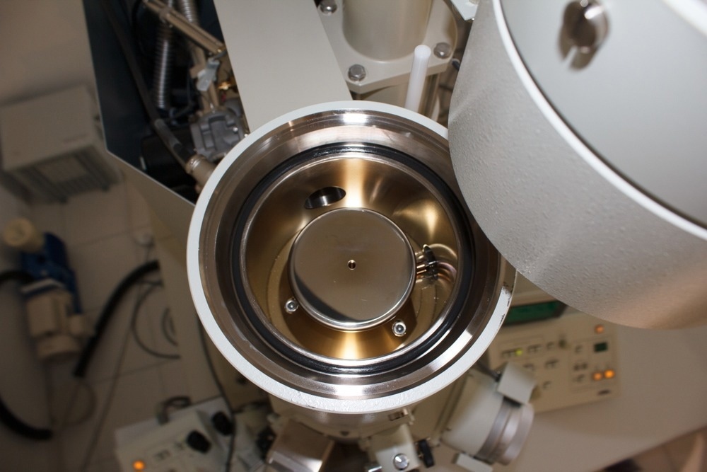
Image Credit: Pvince73/Shutterstock.com
Transmission Electron Microscopy (TEM)
Transmission electron microscopy (TEM) is one of the most common experimental implementations of electron microscopy. With sub-Angstrom spatial resolutions being achievable, TEM can be used to image single atoms on a surface.2
TEM experiments are defined by the geometry of the sample and the detector to the incident electron beam. In TEM, the bright electron beam passes directly through the sample and is detected. The change in the attenuation of the incident electron beam is used to work out the transmission properties of the sample. The incident electron beam can be rastered across the sample to provide spatial information.
Detection of the electrons can either be done through pixel detectors that directly detect the electron beam3 or through using scintillator screens combined with cameras, where the electron charge is converted into an optical signal that can be recorded. Detector design for electron microscopy can be very challenging as indirect detectors tend to have poor quantum efficiencies due to inefficiencies in the conversion process. While more sensitive, direct electron detectors need to be incredibly radiation hard to withstand the damage caused by the electron beam.
TEM images are typically flatter, 2D-like images compared to other electron microscopy methods, such as scanning electron microscopy. Very thin (usually < 150 nm) layers of the sample are used to allow the electron beam to pass through to the detector underneath. With the right sample preparation methods, TEM can be used to image not just the surface of samples but the inner material and allow for the reconstruction of the 3D structure.
Typical examples of applications of TEM include nanomaterial characterization as well as the imaging of biological samples, including tissues.4 The high spatial resolution makes it possible to distinguish small differences in the structure of bacterial cell walls, making TEM a useful diagnostic technique. TEM has proved an important tool in characterizing catalysts and nanoparticle structures.
In Situ Measurements
‘Static’ experiments with limited time resolution record a single image of a sample. For simple characterization experiments, static images may be sufficient to identify parameters such as particle sizes and atomic arrangements. However, most processes in materials science, chemistry and the life sciences involve some kind of dynamical behavior – where the characteristics and properties of the system evolve in time. Often, many key scientific questions revolve around how the sample responds to some stimulus – whether this is the application of a deforming force, light or a change in temperature.
Such in situ measurements have proved very powerful tools for studies of electrochemical systems such as batteries and catalysts, in particular capturing the charge and discharge processes of Si anodes, the resulting volume expansion during lithiation and how this results in battery failure.5 While sample damage does prove a challenge for making TEM measurements of many materials and sometimes necessitates particular sample preparation of cryogenic measurement conditions, many samples can now be measured under pseudo-operational conditions.
While the nanoscale models are not quite the full working conditions of a real battery of fuel cell, developments for in situ TEM holders have made a range of measurements possible for capturing morphology changes and electrode dynamics.
Time-resolution
Many dynamical processes occur on relatively slow timescales, over numbers of seconds or minutes. As there are often limiting factors on how long samples can be exposed to electron beams, achieving the fastest data acquisition rates possible is important to avoid sample damage that may complicate processes. Capturing such dynamical processes also means being able to acquire TEM images on timescales comparable to or shorter than the dynamics of interest.
Many processes in catalysis and chemistry, though, occur on much shorter timescales than seconds. The motion of nuclei in most samples tends to take place on the picosecond to femtosecond timescale, which poses a real challenge for measurements. However, capturing such motions and electronic structure changes in samples is crucial for understanding the early steps in catalysis or how samples interact with stimuli such as light.
One approach has been to find ways to perform stroboscopic measurements with TEM, where the sample is either exposed to external stimuli or not. Then the time-evolution is probed by using pulsed electron imaging. While challenging, femtosecond time resolutions are already achievable with such techniques and they have been used to capture phenomena such as photon-polariton wave packet dynamics in 2D materials.6
Advancements in electron microscopy instrumentation on both the electron sources and detection side have been essential to realizing the development of time-resolved electron microscopies with such short-time resolutions. Improvements in sample holder design have also been essential for expanding the utility of in situ measurements, particularly for battery science where TEM is becoming a highly common technique.
References and Further Reading
Alcorn, F. M., Jain, P. K., & van der Veen, R. M. (2023). Time-resolved transmission electron microscopy for nanoscale chemical dynamics. Nature Reviews Chemistry. doi.org/10.1038/s41570-023-00469-y
Smith, D. J. (2008). Ultimate resolution in the electron microscope? Materials Today, 11, pp. 30–38. https://doi.org/10.1016/S1369-7021(09)70005-7
Tate, M. W., Purohit, P., Chamberlain, D., Nguyen, K. X., Hovden, R., Chang, C. S., Deb, P., Turgut, E., Heron, J. T., Schlom, D. G., Ralph, D. C., Fuchs, G. D., Shanks, K. S., Philipp, H. T., Muller, D. A., & Gruner, S. M. (2016). High Dynamic Range Pixel Array Detector for Scanning Transmission Electron Microscopy. Microscopy and Microanalysis, 22(1), pp. 237–249. https://doi.org/10.1017/S1431927615015664
Arenal, F. L., A., D., & R., M. (2015). Advanced transmission electron microscopy. Springer
Zhang, C., Firestein, K. L., Fernando, J. F. S., Siriwardena, D., von Treifeldt, J. E., & Golberg, D. (2020). Recent Progress of In Situ Transmission Electron Microscopy for Energy Materials. Advanced Materials, 32(18), pp. 1–19. https://doi.org/10.1002/adma.201904094
Kurman, Y., Dahan, R., Sheinfux, H. H., Wang, K., Yannai, M., Adiv, Y., Reinhardt, O., Tizei, L. H. G., Woo, S. Y., Li, J., Edgar, J. H., Kociak, M., Koppens, F. H. L., & Kaminer, I. (2021). Spatiotemporal imaging of 2D polariton wave packet dynamics using free electrons. Science, 372(6547), pp. 1181–1186. https://doi.org/10.1126/science.abg9015
Disclaimer: The views expressed here are those of the author expressed in their private capacity and do not necessarily represent the views of AZoM.com Limited T/A AZoNetwork the owner and operator of this website. This disclaimer forms part of the Terms and conditions of use of this website.