Graphene is often considered a ‘wonder material’ for electronics applications.1 However, while graphene has been proposed as a foundation for making advanced electronics that can be highly multifunctional, deformable and scaled to very small sizes, development can be challenging. In this article, the advantages of applying transmission electron microscopy (TEM) to graphene-based advanced electronics is discussed.
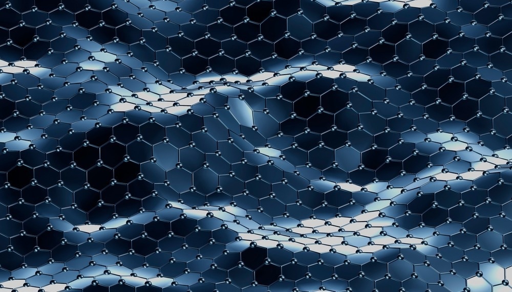
Image Credit: Icruci/Shutterstock.com
In its most basic form, graphene is a two-dimensional (2D) material.2 Composed purely of carbon, graphene sheets are atomically thin in one dimension but have a periodically repeating unit cell in the other. A typical graphene sample has a unit cell that consists of two carbon atoms, separated by approximately 1.42 Å, with an overall unit cell dimension of 2.46 Å.3
What makes graphene a ‘wonder material’ is that the atomic structure means that it has many electrical properties that differentiate it from typical bulk carbon samples, including exceptionally high electron mobility. This, combined with the ability to create thin, flexible graphene sheets and the very high thermal conductivity of graphene, have made it an excellent candidate for next-generation transistors.4
Advanced Electronics
Now, some current advanced electronics applications of graphene include everything from electronic tattoos to miniaturized transistors for advanced logic circuits.5,6 Some of these applications are also focusing on ways to simplify the production of graphene and make low-cost synthesis methods readily available, including using fairly simple copper-polymer substrates for the growth of graphene materials.6
One of the challenges of such ‘do it yourself’ methods that are accessible outside of specialized laboratory conditions and equipment is that it can be somewhat difficult to control the morphology of the samples that are grown in this way.6 For example, potentially unwanted nanoscroll features can only be removed through more complex plasma cleaning processes.
Another challenge for many synthesis methods on all levels of complexity is identifying whether a sample has the necessary morphology for the application. Often in 2D or 3D materials, a particular morphology is chosen to tune the material properties for the desired application.1 However, it is not always obvious or easy to identify by simple visual inspection or testing of the sample whether the graphene morphology is the correct one or not.
TEM
The identification and profiling of graphene samples and their morphology is so challenging because this often requires the visualization of structures on the nanometer length scales. Many standard optical microscopy techniques struggle to achieve the necessary spatial resolution level owing to the diffraction limit of visible light.
Without more specialist superresolution techniques for optical microscopy, one of the main methods for the characterization and analysis of graphene samples has been the family of electron microscopy methods.
Transmission electron microscopy (TEM) can achieve sub-Angstrom spatial resolutions and is, therefore, commonly used for the visualization of the morphology and composition of 2D materials like graphene.7,8 TEM can be used to assess either the overall structure of a more complex 3D graphene-based material or whether there are any defect sites present that may have a dramatic effect on the optical or electronic properties of the graphene samples.
Defects are localized imperfections in the unit cell, and the deliberate introduction of defects into materials is a common approach for tuning the overall material properties.9 Graphene can have a series of natural defects that occur when the carbon atoms that are bonded together rotate by ninety degrees relative to the midpoint of their bonds.10 While this rotation is highly energetically hindered, certain graphene manufacturing processes can deposit sufficient energy in the material to allow such sites to form.
TEM can be used to identify and characterize defect sites with its ability to visualize single atomic structures. This means that TEM is often used in conjunction with the development of new material growth processes to understand how changing parameters such as the temperature affects the overall morphology of the graphene layers being formed and the presence of any defect sites.
New Materials
Graphene-based technologies are undergoing intensive research and development. One of the key hopes for graphene as a material is the very high thermal conductivity will make it possible to make smaller transistors.
Over recent decades, the explosion in available computing power has been driven by the ability to fit more transistors onto a single chip of the same size. However, silicon-based transistors have now reached the limit of what dimensions can be achieved without finding new innovations in how to deal with the heat load, which causes noise in the transistor readout and additional problems.
Graphene-based electronics are one possible solution and may also offer an attractive prospect for avoiding many of the recent shortages of silicon-based chips for devices. However, some of the next steps are finding ways to make affordable devices that can be scaled up in terms of production. There are many promising prototype electronics based on graphene, such as graphene flake detectors, but there is still work to be done to make graphene as mainstream in the electronics industry as silicon.
References and Further Reading
Le Ferrand, H., Chabi, S., & Agarwala, S. (2020). 3D Assembly of Graphene Nanomaterials for Advanced Electronics. Advanced Intelligent Systems, 2(5), 1900151. https://doi.org/10.1002/aisy.201900151
Novoselov, K. S., Geim, A. K., Morozov, S. V., Jiang, D. E., Zhang, Y., Dubonos, S. V., ... & Firsov, A. A. (2004). Electric field effect in atomically thin carbon films. Science, 306(5696), 666-669. https://doi.org/10.1126/science.1102896
Yang, G., Li, L., Lee, W. B., & Ng, M. C. (2018). Structure of graphene and its disorders : a review. Science and Technology of Advanced Materials, 19(1), 613–648. https://doi.org/10.1080/14686996.2018.1494493.
Yan, Z., Nika, D. L., & Baladin, A. A. (2015). Thermal properties of graphene and few‐layer graphene applications in electronics. IET Circuits, Devices and Systems, 9(1), 4–12. https:/doi.org/10.1049/iet-cds.2014.0093
Naghibi, S., Kargar, F., Wright, D., Huang, C. Y. T., Mohammadzadeh, A., Barani, Z., Salgado, R., & Balandin, A. A. (2020). Noncuring Graphene Thermal Interface Materials for Advanced Electronics. Advanced Electronic Materials, 6(4), 1–9. https://doi.org/10.1002/aelm.201901303
Kireev, D., Ameri, S. K., Nederveld, A., Kampfe, J., Jang, H., Lu, N., & Akinwande, D. (2021). Fabrication, characterization and applications of graphene electronic tattoos. Nature Protocols, 16(5), 2395–2417. https://doi.org/10.1038/s41596-020-00489-8
Smith, D. J. (2008). Ultimate resolution in the electron microscope? Materials Today, 11, 30–38. https://doi.org/10.1016/S1369-7021(09)70005-7
Chang, Y., Han, H. N., & Kim, M. (2019). Analyzing the microstructure and related properties of 2D materials by transmission electron microscopy. Applied Microscopy, 49, 10. https://doi.org/10.1186/s42649-019-0013-5
Ping, Y., & Smart, T. J. (2021). Computational design of quantum defects in two-dimensional materials. Nature Computational Science, 1, 646–654. https://doi.org/10.1038/s43588-021-00140-w
Bhatt, M. D., Kim, H., & Kim, G. (2022). Various defects in graphene: a review. RSC Advances, 12(33), 21520–21547. https://doi.org/10.1039/d2ra01436j
Disclaimer: The views expressed here are those of the author expressed in their private capacity and do not necessarily represent the views of AZoM.com Limited T/A AZoNetwork the owner and operator of this website. This disclaimer forms part of the Terms and conditions of use of this website.