The STEMx® system can effectively enhance the current Gatan in-situ camera’s 4D STEM diffraction capabilities.
The new STEMx system acquires data by synchronizing hardware with Gatan’s in-situ cameras. STEMx uses the excellent spatial and temporal resolution of the K3® IS, ClearView®, Metro®, Rio® IS, and Stela®* cameras to enable a broad range of 4D STEM experiments, such as strain mapping, indexing, orientation mapping, virtual apertures, and differential phase contrast.
Features
- Large sample areas can be scanned with great diffraction space resolution
- Use the current Gatan in-situ camera to control new 4D STEM applications
- In less than 10 minutes, users can assess initial information
- Automate workflow for sophisticated applications
The user can view and alter all of the data in a 4D STEM diffraction cube, such as diffraction planes or individual diffraction patterns at each pixel location, with a single, interactive DigitalMicrograph® 3 display once a diffraction pattern has been generated for each data point.
By adopting data size reduction techniques like four-dimensional binning, spatial domain sub-sampling, or picking a small area of interest, STEMx can then handle these enormous datasets in minutes. Users using DigitalMicrograph 3 can quickly study and evaluate results under the microscope and decide whether to adjust the acquisition parameters or acquire a fresh dataset by merging acquisition and analysis.
*Stela utilizes DECTRIS hybrid-pixel technology
4D STEM Diffraction Data Cube Collected Using the Stela Camera and STEMx System
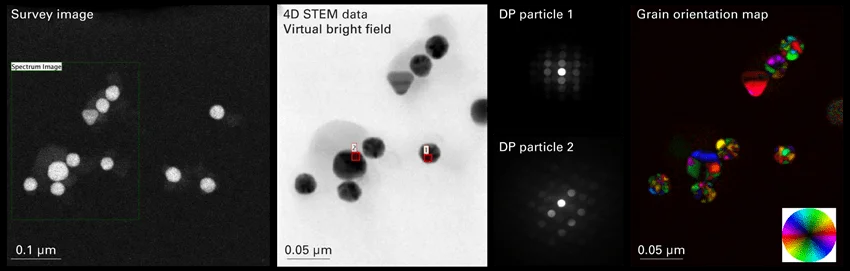
4D STEM diffraction data cube. A 4D STEM diffraction data cube was collected using the Stela camera and STEMx system. Specimen: Au nanoparticles. Scan area: 176 × 218 pixels, Diffraction image size: 256 × 256 pixels. Dwell time: 5 ms. Color map showing grain orientations classified based on the angular position of the maximum diffraction peak per probe position using a DigitalMicrograph script. Image Credit: Gatan, Inc.
Differential Phase Contrast (DPC) Maps of Pyrochlore Oxide Specimen Calculated from a 4D STEM Dataset
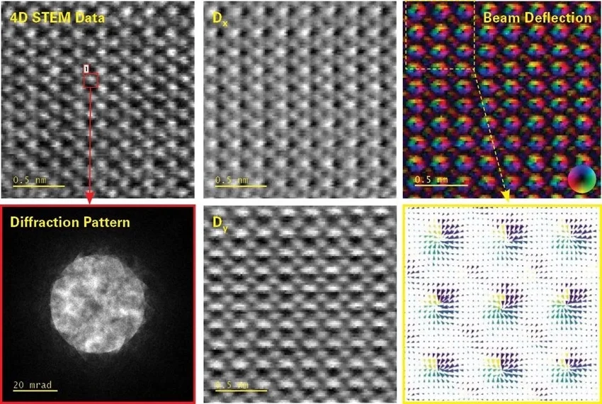
DPC maps of pyrochlore oxide specimen. Differential phase contrast (DPC) maps were calculated from a 4D STEM dataset acquired at atomic resolution from a pyrochlore oxide specimen using the GIF Continuum® K3 equipped with STEMx and the in-situ option. This energy-filtered 4D dataset included approximately 12,100 diffraction patterns and was collected in electron counting mode in <20 seconds. Image Credit: Gatan, Inc.
Demonstrating Differential Phase Contrast (DPC) Imaging in DigitalMicrograph
Differential Phase Contrast in DigitalMicrograph: Electric Field Measurement
DPC in DigitalMicrograph. This video demonstrates two DPC imaging methods in DigitalMicrograph: Virtual Segmented Detector and Center of Mass (CoM). Video Credi: Gatan, Inc.
Solving the Practical Material Problem of Low Voltage Electron at High Speed by Using Stela
Utilization of low voltage electron diffraction at high speed to solve practical materials problems
Utilization of low voltage electron diffraction at high speed to solve practical materials problems. This webinar shows examples of low-voltage, high-speed electron diffraction experiments using the Gatan Stela, a detector with a high-dynamic range, based on DECTRIS’ fast hybrid-pixel technology, to study subtle structural changes. Video Credit: Gatan, Inc.
A Presentation of Stela Hybrid Pixel Electron Detector for 4D STEM Diffraction
Live Virtual Workshop: Stela Hybrid Pixel Electron Detector for 4D STEM Diffraction
Live Virtual Workshop: Stela Hybrid Pixel Electron Detector for 4D STEM Diffraction. This comprehensive workshop features a presentation, a live microscope demonstration (including 4D STEM data acquisition and processing), and an open Q&A session. Video Credit: Gatan, Inc.
NUANCE Workshop on 4D STEM: Data Processing Using Python
NUANCE Workshop on 4D STEM: Data Processing using Python
NUANCE Workshop on 4D STEM: Data Processing using Python. Webinar is based on demonstrating of 4D STEM by using data processing strategies such as HyperSpy, Pyroscopy, LiberTEM, and many more with the help of steps in management which included 1. Bining 2. Cropping 3. Counting, by Stephaine Ribet from the Department of Material Science and Engineering, Northwestern University. Video Credit: Gatan, Inc.
NUANCE Workshop on 4D STEM: Data Processing in DM
NUANCE Workshop on 4D STEM: Data Processing in DM
NUANCE Workshop on 4D STEM: Data Processing in DM. The workshop has included depicting the 4D STEM data processing in DigitalMicrograph which has assisted in its applications including strain mapping, virtual apertures, DPC, and many more. A brief demonstration by Anahita Pakzad.Video Credit: Gatan, Inc.
NUANCE Workshop on 4D STEM: Fundamentals of Electron Diffraction and 4D STEM
NUANCE Workshop on 4D STEM: Fundamentals of Electron Diffraction and 4D STEM
NUANCE Workshop on 4D STEM: Fundamentals of Electron Diffraction and 4D STEM. The workshop is dedicated to illustrating the fundamentals of electron diffraction and 4D STEM by categorizing into three parts i.e., introduction to CBED, 4D STEM, application in soft/hard interfaces, and soft material by Roberto dos Reis. Video Credit: Gatan, Inc.
Demonstrating Stain Mapping
Strain Mapping with STEMx
Strain mapping. Here, we show how to calculate specimen strain from a 4D STEM nanobeam diffraction dataset in the DigitalMicrograph software. Video Credit: Gatan, Inc.
Elaborating the Steps Involved in DIFPack Tools
Using DIFPack Tools for STEMx Datasets
DIFPack Tools. Here we show how to use DIFPack tools to analyze 2D diffraction patterns and 4D STEM diffraction data cubes. Video Credit: Gatan, Inc.