Imec and Holst Centre have developed stable patterned electrets with feature sizes at least down to 20µm. The technology consists in creating a charged profile in a SiO2/Si3N4 structure by exploiting the difference in energy between the charge traps located in either layer and at their interface. Patterned electret layers can be used for a plurality of technical applications such as micromotors, sensors, actuators and energy scavengers.
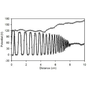 Charge pattern in a SiO2/Si3N4 electret. The top curve shows the charge in a reference 7mm-wide strip. A uniform potential is obtained on lines from 7mm to 20ìm-wide. The electrostatic probe does not resolve narrow lines and shows an average potential.
An electret in its most general meaning is a dielectric material that stores a quasi-permanent electric charge upon its polarization. For a plurality of MEMS applications such as micromotors, transducers and vibration energy scavengers, thin patterned electret layers are required. In these applications, the patterned electret could serve as a high-voltage source with a service life of hundreds of years to replace both the battery and the high-voltage up-converter. However, no technologies have so far allowed the fabrication of stable patterned electret structures with features sizes of a few tens of micrometers. Electrets patterned by using photolithography show rapid charge decay in narrow patterned structures. Imec and Holst Centre have now demonstrated a technology that allows the fabrication of narrow lines and other electret film structures with feature sizes down to 20µm. The patterned electret structures show no dependence of charge retention on line width as measured one year after fabrication.
The technology makes use of a SiO2/Si3N4 electret in which a charged profile is created based on the difference in energy between charge traps located in either layer and at their interface. Stability of charge retention in electrets is indeed related to the charge trap energy: the higher their energy, the longer is the lifetime of charge in electrets. Measurements performed by imec and Holst Centre have shown that interface traps are much deeper than traps observed in either SiO2 or Si3N4. This feature allows the creation of a charge pattern in electrets by selective patterning the first or the second layer e.g. by dry etch. Before patterning, the electrets are protected from the ambient humidity by dehydration of SiO2/Si3N4 and subsequent treatment with vapor hexametildisilazane (HMDS) at 140°C.
The developed process can be used in different microsystem applications. Furthermore, microsystems require packaging, wafer stacking and other high-temperature processes. The technology allows such processes with practically no loss in charge and with no effect of high temperature processes (up to 450°C) on charge retention. It has already been successfully used for the fabrication of an electrostatic energy harvester. Further improvements focus on the development of stable electret patterns with feature sizes down to 1µm, high-potential electrets and improved charge retention in electrets in photolithographic processes.