Researchers at imec and at the Center for Advanced Materials Processing (CAMP) of the Clarkson University in Potsdam, New York (U.S.) have recently started a collaboration to study the fundamentals of CMP processes for novel materials such as Ge or III/V compounds. This study aims to further optimize the CMP processes that are used in the integration of these new materials in IC processing. A first finding on Ge-on-Si wafers is that the oxide removal rate and the Ge roughness are inversely proportional.
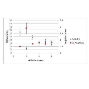 Oxide removal rate and Ge roughness for various slurries: the oxide removal rate and the Ge roughness are inversely proportional.
To further scale IC devices, new materials are called for. Examples are the Ge or III/V compounds that are used as high-mobility channel material. Strained Ge is a very good candidate channel material for pMOS devices, because of its significantly higher mobility. And III/V materials are good candidates for use in nMOS devices. Such strained Ge and III/V compounds can be used, combined with a high-k dielectric as gate oxide, even if they don’t have a stable thermal oxide.
The new materials are integrated on bulk Si wafers after completion of the standard shallow trench isolation (STI). The active Si is removed creating trenches. In these trenches, the high-mobility materials are selectively grown through epitaxial processes. To make sure that there is good edge coverage, the trenches are filled until the high-mobility materials overflow the edges. The resulting surface is rough; CMP processes are needed to remove the overfill and to smoothen the surface.
While the integration of these materials on bulk Si wafers is already ongoing and first CMP processes were developed, there is still a need to better understand the mechanisms for these CMP processes and to further optimize them. Ideally the removal rates would be tunable for Ge and SiO2, on which the CMP process needs to stop. It is critical that the polished Ge surface after CMP is defect free and has a very low roughness (<0.5nm root mean square (RMS)).
Starting with studies for the CMP of Ge and SiGe films, the collaboration between imec and CAMP aims to improve the understanding of the polishing mechanisms for these materials. The common understanding of the mechanism for Ge CMP is the oxidation of Ge by a strong oxidizer followed by abrasion of the oxidized Ge layer by abrasives present in the slurry. Experiments with Ge disks and with Ge-on-Si wafers from imec were done at CAMP to study the influence of different oxidizers at various pH values. A first finding is that the oxide removal rate and the Ge roughness are inversely proportional. Further tests will be done to explore this correlation.