Imec demonstrates the value of its SiGe above-IC MEMS technology platform for improving performance of state-of-the-art MEMS with the development of new MEMS devices. The new devices are a 15µm SiGe micromirror and a grating light valve for high-resolution displays. The devices were realized with imec’s generic CMOS-compatible MEMS process for the monolithic integration of MEMS devices directly on top of CMOS metallization.
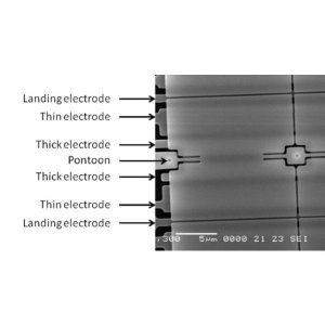 SEM picture of a 15µm SiGe micromirror.
The 15µm micromirror, designed for use in display systems, uses an innovative electrostatic actuation mechanism relying on 6 electrodes. The design enables analog pulse-width modulation (PWM) instead of the binary-weighed PWM of current state-of-the-art MEMS-based micromirrors. This novel actuation mechanism allows display of a large range of grey-scale values, while binary-weighed PWM depends on the number of sub-frames or bit-planes. Using analog PWM thus leads to higher response speed, less image processing hardware and less memory. Moreover, the analog PWM is implemented on the MEMS level instead of on the CMOS level, allowing a simplified electronic circuit.
The second device is a grating light valve, a MEMS reflection grating producing bright and dark pixels in a display system by controlled diffraction of incident light due to electrostatic deflection of microbeams. The grating light valve uses clamped-clamped microbeams which are suspended over an electrode. It can modulate the intensity of the diffracted light when an actuation voltage is applied to half of the beams. Display systems using such a technology provide a high contrast ratio, high resolution and high brightness. Both the mirrors and grating light valves are realized with a 300nm thick SiGe structural layer.
The devices have been realized in the frame of the Flemish Strategic Basic Research (SBO) project Gemini, a collaboration between imec, Ghent University and Katholieke Universiteit Leuven (K.U.Leuven). Imec’s MEMS technology platform, set up in imec’s 200mm fab, to integrate MEMS and its readout and driving electronics on one chip, has been used to design and process the devices. The platform consists of a number of standard modules (CMOS protection layer, MEMS via and poly-SiGe electrode, anchor and poly-SiGe structural layer and a thin-film poly-SiGe packaging module) which can be processed at ~450ºC above standard CMOS. Optional (optical, piezoresistive, probes…) modules can be added, depending on the functionality that is needed. This monolithic approach results in more compact systems with a reduced assembly and packaging cost and a higher performance than current hybrid systems. Companies can get access to this MEMS-technology platform through the imec CMORE service (www.imec.be/cmore).
Imec performs world-leading research in nanoelectronics. Imec leverages its scientific knowledge with the innovative power of its global partnerships in ICT, healthcare and energy. Imec delivers industry-relevant technology solutions. In a unique high-tech environment, its international top talent is committed to providing the building blocks for a better life in a sustainable society. Imec is headquartered in Leuven, Belgium, and has offices in Belgium, the Netherlands, Taiwan, US, China and Japan. Its staff of more than 1,750 people includes over 550 industrial residents and guest researchers. In 2009, imec's revenue (P&L) was 275 million euro.
Imec is a registered trademark for the activities of IMEC International (a legal entity set up under Belgian law as a "stichting van openbaar nut”), imec Belgium (IMEC vzw supported by the Flemish Government), imec the Netherlands (Stichting IMEC Nederland, part of Holst Centre which is supported by the Dutch Government), imec Taiwan (IMEC Taiwan Co.) and imec China (IMEC Microelectronics (Shangai) Co. Ltd.).