Imec and KLA Tencor have established a metrology method for optimizing the etch rate uniformity (ERU) in a transformer coupled plasma (TCP) reactor. The proposed metrology method makes use of PVx2 sensor wafers. For ion-assisted etch processes, the use of this PVx2-based method for ERU tuning results in lot-turn time savings of up to 80% compared to conventional etch rate uniformity tests.
Uniformity control in plasma etch processes and process stability requirements are major challenges in IC high-volume production and they are becoming more aggressive for each new technology node. Therefore, the availability of a metrology suited for predicting and tuning the etch rate uniformity has become a key element for effective process optimization. Imec and KLA Tencor have now demonstrated that PlasmaVoltTM X2 (PVx2) sensor wafers, for some specific process etch chemistries, offer a fast and reliable way of ERU tuning and can significantly improve lot-turn time savings.
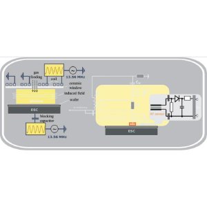 Principles of plasma generation and an equivalent electrical representation of PVx2 in a TCP reactor: the transformer coupled capacitive tuning (TCCT) parameter is able to specify the portion of power applied to center vs. outer segment of the top coil. The higher the TCCT setting, the more power is directed towards the center segment of the TCP coil.
With a PVx2 sensor wafer, the RF current that is passing through each of the surface-mounted capacitive detectors is measured and linked to the local plasma impedance. The researchers performed their experiments in a transformer coupled plasma reactor and used the transformer coupled capacitive tuning (TCCT) parameter to change the etch rate uniformity distribution. Experiments to study the influence of this parameter were carried out on blanket wafers (poly-Si and SiO2) as well as on patterned wafers with 20nm half-pitch back-end-of-line interconnect trenches (SiOC, BARC, and SiN etch steps). For various typical etch chemistries and different settings of the TCCT parameter, the RF signals recorded by the PVx2 sensor wafers were compared with conventional etch rate uniformity measurements. The latter included thickness measurements (in case of blanket wafers) and critical dimension (CD) uniformity measurements (in case of patterned wafers).
For blanket wafers, the wafer sensor provides an adequate tool to predict etch rate uniformity trends in a transformer coupled plasma reactor for etching processes that require ion assistance, such as SiO2 etching. For these processes, it has been shown that lot-turn time savings of 80% or more can be achieved when compared to single-use blanket wafer etch rate uniformity tests. For other types of processes that involve e.g. spontaneous chemical reactions (like for poly-Si etching involving fluorine-based chemistries), the method turns out to be less effective.
For the 20nm half-pitch wafers, a good correlation of the sensor wafer and CD uniformity data was found for SiOC and BARC etching, but not for the SiN etch step. For SiN etching, a CH3F/O2 plasma is used that is highly selective towards the masking material, and this more chemistry-dominated mechanism most likely explains the observed discrepancy.
These results have been presented at the 21st Annual IEEE/SEMI Advanced Semiconductor Manufacturing Conference (ASMC 2010).