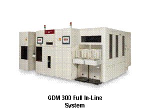
Okamoto announced today that SEMATECH, the global consortium of chip-makers, has selected Okamoto's GDM300 Backgrinder for processing Through Silicon Via (TSV). The System, a High-Precision wafer thinning tool, will be installed in SEMATECH's 3D R and D Center at the College of Nanoscale Science and Engineering's (CNSE) world-class Albany NanoTech Complex.
After the grind process, stress release is achieved by dual high speed scanning polishing heads able to achieve +/- 5% non-uniformity. Improved die strength is achieved by simultaneously utilizing CMP and water polish. An integrated edge trimmer eliminates edge chipping and improves yield. Non-contact measurement devices enable precision thickness accuracy.
Sitaram Arkalgud, SEMATECH's 3D program director, added, "SEMATECH's 3D program is focused on enabling the manufacturability of 3D interconnects, and one of our key infrastructure requirements is a system that provides an integrated process that allows our engineers to identify and quantify the technical challenges of thinning wafer pairs to achieve damage-free bonds."
Richard Brilla, CNSE's Vice President for Strategy, Alliances and Consortia, said, "The addition of Okamoto's wafer-thinning tool will support the advanced work being done through SEMATECH's 3D program, as well as the state-of-the-art capabilities at CNSE's Albany NanoTech, which are enhancing the industry's efforts to manufacture increasingly complex nanoscale devices."
The system is designed for thin wafer applications such as TSV, bonded wafers, SOI, and MEMS. Also available optionally in a full line system for single wafer thinning are dicing frame mounting, UV curing and detaping of protective tape. DAF tape can also be applied in lieu of standard dicing tape.