Apr 13 2017
 Cross-section scanning electron microscopy image after hydrogen silsesquioxane patterning, sequential infiltration synthesis and removal of initiated chemical vapor deposition topcoat and organic components. (Image by Hyo Seon Suh / University of Chicago)
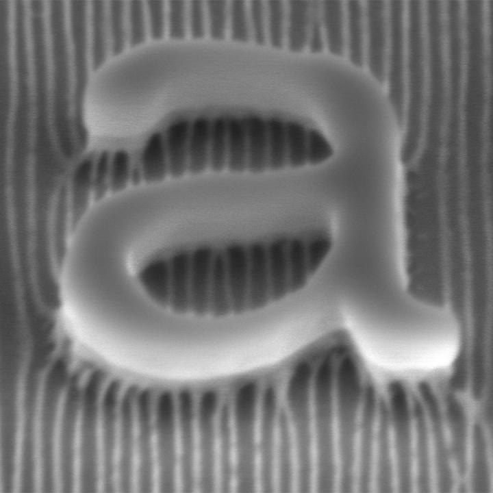
In order to enable faster working of the chips in computers and smartphones, the size of the wires and circuits through which signals are transmitted has to be reduced considerably. While miniaturizing these wires, researchers had to undergo an expedition to nearly the atomic level. At present, researchers have started to deal with as well as overcome specific barriers in physics that hinder the making of very small wires.
A new research by a group of scientists from the U.S. Department of Energy’s Argonne National Laboratory (DOE), the University of Chicago, and MIT has led to an innovative method for developing the thinnest wires of the world by means of a process that allows mass production by using standard equipment.
Referred to as templated assembly (or directed self-assembly), the new process is an uncomplicated and highly cost-efficient method to produce nanowires that have a width less than 10 nm, with a thickness of nearly 100 atoms.
The self-assembling materials are huge molecules called as block copolymers, which are the two-ended giants in the field of chemistry. One of their ends is water-loving, and the other end is water-hating. When the material is heated, the ends impulsively form extremely uniform structures at the molecular level.
However, the block copolymers themselves form a pattern resembling a piece of brain coral or a fingerprint. This pattern does not hold good for producing functional nanowires. This pattern can be transformed into a highly ordered one by using chemically patterned templates.
Earlier techniques for producing tiny ordered nanostructures involved the use of high-cost specialized optics for directing extreme wavelengths of electron beams or light for line-by-line writing of patterns. By using the innovative method invented in this study, a chemical pattern is developed as a template by means of the same tools at a comparatively low resolution, and subsequently, the template is filled in for producing high-resolution patterns from a self-assembling material.
In the case of block copolymer systems with very high resolution, a “topcoat” is normally added during the technique, which restricts the manner in which the block copolymers get self-assembled, thereby constraining them into an ordered, regular structure that is perpendicular to the surface on which they are developed.
Think of it like baking a cake. Without a mold for the cake, it can bake in a shape you don’t want it to bake. Having the mold gives it that shape that you want. The mold creates boundary conditions needed to define the shape you want. The topcoat and underlying lithographic pattern work together to guide the formation of the nanostructure and provide the morphology we want.
Leonidas Ocola, Argonne nanoscientist & co-author of the study
Despite the fact that researchers have been aware of self-assembling materials in nanomanufacturing for some time now, patterns for dense arrays of tiny wires can be produced by using block copolymers that have topcoat.
A systems-level understanding of the template, topcoat and self-assembling block copolymer is the key to the whole process—you need to find a way to induce the block copolymer film to assembly into desired architectures for manufacturing, and be able to transfer the pattern of the block copolymer into the actual device materials, such as semiconducting silicon wires or conducting copper wires
Paul Nealey, author & Brady W. Dougan Professor in Molecular Engineering at the Institute for Molecular Engineering at the University of Chicago
The fact that the topcoat polymer layer does not have to be removed before performing the pattern transfer steps, and that subsequent layers could be patterned on the topcoat, various types of complex patterns, such as those required for interconnections of a microchip, can be built by using the system.
Majority of the microchip manufacturing facilities employ prevalent lithographic techniques, and the chemical vapor deposition process for developing the topcoat is a well-perceived additional process that can be easily performed. Consequently, the new technique can be performed very easily than other proposed techniques for producing finer lines.
Using the new technique:
You wouldn’t need to change all those machines and everything that’s involved are well-known materials.
Karen Gleason, co-author & MIT associate provost and Alexander and I. Michael Kasser Professor of Chemical Engineering
The outcomes of the research have been published in the journal Nature Nanotechnology on 27 March in an article titled, “Sub-10-nm patterning via directed self-assembly of block copolymer films with a vapour-phase deposited topcoat.” The electron-beam lithography and the x-ray scattering experiments were carried out at Argonne’s Advanced Photon Source and Center for Nanoscale Materials, both of which are DOE Office of Science User Facilities.
The study was also supported by the National Science Foundation and the U.S. Army Research Office, by means of MIT’s Institute for Soldier Nanotechnologies.