Oct 23 2017
Developments in the field of nanoelectronics, specifically the application of nanotechnology to electronic components, has been powered up by the ever-expanding requirement to reduce the size of electronic devices in an attempt to develop smaller, smarter, and faster gadgets such as memory storage devices, computers, medical diagnostic tools, and displays.
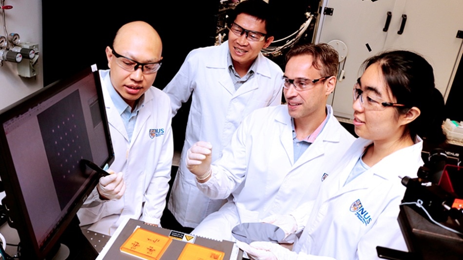 A research team led by Associate Professor Christian Nijhuis from the Department of Chemistry at the NUS Faculty of Science (second from right) has recently invented a novel “converter” that can harness the speed and small size of plasmons for high frequency data processing and transmission in nanoelectronics. Credit: National University of Singapore
Although the majority of current electronic devices are based on photonics (i.e. using photons to convey information), in general, the size of the photonic element is large, thereby considerably restricting the use of photonics in various state-of-the-art nanoelectronics systems.
Plasmons, which are waves of electrons that move along the surface of a metal after it is struck by photons, holds great promise for disruptive technologies in nanoelectronics. With respect to speed, they are comparable to photons—as they also travel at the speed of light—however they are much smaller in size. This distinctive characteristic of plasmons makes them optimal for combining with nanoelectronics. Yet, previous efforts in using plasmons as information carriers were not very fruitful.
In order to bridge this technological void, a team of scientists from the National University of Singapore (NUS) has recently developed an innovative “converter” with the ability to put the small size and speed of plasmons to good use in high-frequency data processing and transmission in nanoelectronics.
“This innovative transducer can directly convert electrical signals into plasmonic signals, and vice versa, in a single step. By bridging plasmonics and nanoscale electronics, we can potentially make chips run faster and reduce power losses.” elucidated Associate Professor Christian Nijhuis from the Department of Chemistry at the NUS Faculty of Science, who headed the researchers behind the latest advancement.
Our plasmonic-electronic transducer is about 10,000 times smaller than optical elements. We believe it can be readily integrated into existing technologies and can potentially be used in a wide range of applications in the future.
Associate Professor Christian Nijhuis from the Department of Chemistry at the NUS Faculty of Science
The finding was first published on September 29, 2017 in the Nature Photonics journal.
From electricity to plasmons in one single step
In the majority of plasmonics methods, plasmon excitation occurs as a two-step process in which first electrons are used to produce light, which in turn excites plasmons. For a single-step conversion of electrical signals into plasmonic signals and vice versa, the NUS researchers adopted a process known tunneling, where electrons move from one electrode to the other, and in the process excite the plasmons.
“The two-step process is time-consuming and inefficient. Our technology stands out as we provide a one-stop solution for the conversion electrical signals to plasmonic signals. This can be achieved without a light source, which requires multiple-steps and large optical elements, complicating integration with nanoelectronics. Based on our lab experiments, the electron-to-plasmon conversion has an efficiency of more than 10 per cent, more than 1,000 times higher than previously reported,” explained Assoc Prof Nijhuis, who is also from the NUS Centre for Advanced 2D Materials and NUS Nanoscience and Nanotechnology Institute.
The revolutionary research was performed in cooperation with Dr Chu Hong Son from the Institute of High Performance Computing under the Agency for Science, Technology and Research.
Industry partnership and further studies
Four patents have been filed on behalf of the team for their invention. They are also cooperating with industry partners to incorporate the plasmonic-electronic “converters” in prevalent technologies.
The team is looking forward to perform further analyses to decrease the size of the device to enable it to function at considerably greater frequencies. The researchers are also striving to integrate more efficient plasmonic waveguides into the transducers for ensuring better performance.