Jan 25 2019
An innovation in fabricating atom-thin processors has been reported by an international team of scientists. This discovery could have extensive influence on nanoscale chip manufacture and in labs worldwide where researchers are studying 2D materials for ever-smaller and -faster semiconductors.
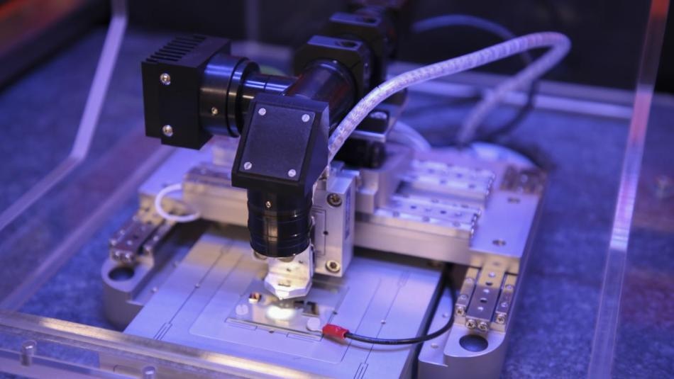 Researchers in the PicoForce Lab modified hot-probe equipment called NanoFrazor by SwissLitho to invent a new process of fabricating 2D semiconductors. Here, the equipment patterns a one-atom-deep layer of molybdenum disulfide with electrodes. (Image credit: New York University Tandon School of Engineering)
The research team, guided by New York University Tandon School of Engineering Professor of Chemical and Biomolecular Engineering Elisa Riedo, reported the research outcomes in the most recent issue of Nature Electronics.
They prove that lithography performed using a probe heated to more than 100 °C outdid regular techniques for fabricating metal electrodes on 2D semiconductors such as molybdenum disulfide (MoS2). Such transitional metals belong to a group of materials that researchers believe may displace silicon for atomically small chips. The team’s new fabrication technique—known as thermal scanning probe lithography (t-SPL)—offers many benefits over present-day electron beam lithography (EBL).
Firstly, thermal lithography greatly enhances the quality of the 2D transistors, offsetting the Schottky barrier, which obstructs the flow of electrons at the intersection of metal and the 2D substrate. Furthermore, in contrast to EBL, the thermal lithography enables chip designers to easily image the 2D semiconductor and subsequently pattern the electrodes where needed.
Similarly, t-SPL fabrication systems promise considerable preliminary savings as well as operational costs: They radically lower power consumption by working in ambient conditions, removing the need to create high-energy electrons and to produce an ultra-high vacuum. Lastly, this thermal fabrication technique can be effortlessly scaled up for industrial fabrication by using parallel thermal probes.
Riedo voiced hope that t-SPL will remove most fabrication out of scarce clean rooms—where scientists must contend for time with the expensive equipment—and into individual laboratories, where they might quickly promote materials science and chip design. The instance of 3D printers is an appropriate analogy: In the future, these t-SPL tools with sub-10-nm resolution, operating on standard 120-V power in ambient conditions, could become equally ubiquitous in research labs like hers.
“Patterning Metal Contacts on Monolayer MoS2 with Vanishing Schottky Barriers Using Thermal Nanolithography” has been published in the January 2019 edition of Nature Electronics with a “News & Views” analysis.
Riedo’s research on thermal probes goes back to more than 10 years, first with IBM Research–Zurich and then SwissLitho, founded by former IBM researchers. A process based on a SwissLitho system was formulated and used for this study. She started investigating thermal lithography for metal nanomanufacturing at the City University of New York (CUNY) Graduate Center Advanced Science Research Center (ASRC), working along with co-first-authors of the paper, Xiaorui Zheng and Annalisa Calò, who are now post-doctoral researchers at NYU Tandon; and Edoardo Albisetti, who worked on the Riedo team with a Marie Curie Fellowship.
Authors who contributed include NYU Tandon Assistant Professor of Electrical and Computer Engineering Davood Shahrjerdi; NYU Tandon doctoral students Xiangyu Liu and Abdullah Sanad M. Alharbi; Columbia University’s Ghidewon Arefe, James Hone, Brian S. Lee, and Michal Lipson; Sungkyunkwan (Korea) University’s Xiaochi Liu and Won Jong Yoo; SwissLitho’s Martin Spieser; the Japanese National Institute of Materials Science’s Takashi Taniguchi and Kenji Watanabe; Italy’s National Research Council’s Carmela Aruta; and the Swiss École Polytechnique Fédérale de Lausanne’s Alberto Ciarrocchi and Andras Kis.
The study was supported by the U.S. Army Research Office, the Office of Basic Energy Sciences of the U.S. Department of Energy, the National Science Foundation, and the European Union’s Horizon 2020 Research and Innovation Programme.