The development of structurally and thermally sound marking stamps based on phase-separated nanostructures (PSNs) for nanoimprint lithography (NIL) systems was reported in an article recently published in the Advanced Materials Technologies journal.
Study: A Self-Assembly Method for Tunable and Scalable Nano-Stamps: A Versatile Approach for Imprinting Nanostructures. Image Credit: Ersan Uzunoglu/Shutterstock.com
Researchers established that these nanoimprint stamps are readily adjustable and expandable through alteration of the composition of the homopolymer hybrid-polymer combination and the application settings. Through the interaction of these parameters, component sizes in PSN may range between a few μm to 100 nm.
Nanoimprint Lithography
NIL is regarded as an appealing method for producing microscale or nanoscale structures to improve the efficiency of a broad range of materials and equipment, such as flexible electronic devices, anti-counterfeit labeling, and antimicrobial treatments.
Generally, NIL employs a structured stamp composed of either hard or soft substances for transferring the pattern to the basal layer via mechanical deformation. As a result, the nanoimprint stamp specimen is anticipated to be relatively hard throughout the NIL procedure.
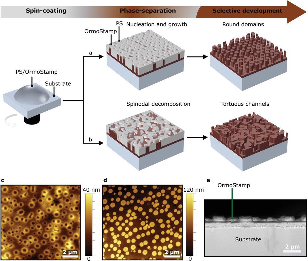
PS/OrmoStamp blend enables the direct patterning of OrmoStamp material via SA. A schematic illustration of the formation of spin-casted PSN via a) nucleation and growth, and b) spinodal decomposition mechanism at room temperature. Afterward, the PS matrix is selectively etched using O2 plasma treatment. AFM images of the PSN c) before and d) after O2 plasma treatment of a sample prepared using PS/OrmoStamp with a 3:1 ratio in the solvent toluene, with a concentration of 35 mg mL−1. A spin-casting speed of 1500 rpm is used for producing the PSN. The Ormostamp nanopillar top surface is represented by a black color in (c) and with a bright color in (d). e) Cross-sectional SEM image of the Ormostamp nanopillars in (d). Image Credit: Donie, Y. J., et al
Fabrication of the Imprinting Stamps
To decrease the costly stamp strain based on rigid materials, nanoimprint stamps composed of pliable and soft materials, commonly consisting of polymers or polymer-ceramics, have since been created. Additionally, these nanoimprint stamp constituents may eliminate flaws on an embossed region via localized deformation around undesired particles.
The production of the nanoimprint stamp is critical and greatly influences the efficiency of the NIL procedure regardless of the constituent materials utilized. Thus far, rigid material nanoimprint stamps have been successfully manufactured by integrating a range of top-down lithography processes such as e-beam, photo-, laser interference, and colloidal lithography with wet/dry etching or electrodeposition. In certain circumstances, these operations are costly and time-consuming to perform, posing a barrier to the commercial viability of NIL-based products.
Bottom-up lithography approaches, such as a self-assembly approach (SA) on the basis of phase-separated polymeric mixes, may provide a viable way around this constraint. As a result, its advantages are comparable to those of NIL.
That being said, traditional SA is often reliant on polymeric materials with low glass transition temperature levels. As an elevated temperature is often needed while the imprinting stage takes place, the coefficient of thermal expansion is critical in the NIL method. In-plane stamp deformation or increased stress during the cooling period are caused by nanoimprint stamps' thermal instability. As a result, it impacts the design integrity and accuracy of imprint registration. These challenges must be solved if the SA advantages are to be translated into a commercially feasible NIL production method.
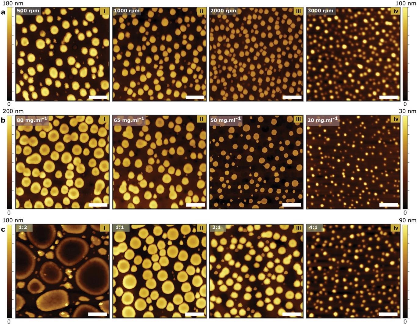
Influence of the ink composition and the deposition parameters on the resulting morphology of the PSN. a) AFM images of Ormostamp nanopillars fabricated using four different spin-casting speeds: i) 500, ii) 1000 iii) 2000, and iv) 3000 rpm. A PS/OrmoStamp = 3:1 blend in toluene solvent with a concentration of 35 mg mL−1 was used. b) AFM images of Ormostamp nanopillars prepared with different concentrations of PS/Ormostamp with a 3:1 weight ratio in toluene: i) 80, ii) 65, iii) 50, and iv) 20 mg mL−1. A spin-casting speed of 1500 rpm is used to produce the PSN. c) AFM images of Ormostamp nanopillars prepared with different weight-ratios of PS and OrmoStamp in the blend, PS/OrmoStamp weight ratio: i) 1:2, ii) 1:1, iii) 2:1, and iv) 4:1. The blends were dissolved in toluene with a concentration of 35 mg mL−1 and spin-casted at 1500 rpm. All AFM images were acquired after the selective etching of the PS matrix using O2 plasma. The scale bar represents 2 μm in all AFM images. The scale bar on the left and right sides of the AFM images represents the samples’ height profiles in (i–iii) and (iv), respectively. Image Credit: Donie, Y. J., et al
Findings of the Study
The self-assembly approach of polymeric mix phase separation provides a diverse foundation for manufacturing readily controllable periodic patterning for nanoscale photonics applications. This work used SA to develop a robust and repeatable manufacturing process for PSN-based nanoimprint stamps with configurable physical characteristics for NIL.
To fulfil the stringent procedural demands, a novel ink-formulation technique comprising of the homopolymerized-PS and the synthetic-organic hybrid polymer – OrmoStamp is created.
The PSN structural characteristics were tweaked across different substrates by interacting with the original polymeric mix recipes and procedural parameters. Because of the nature of the constituent, the resultant PSN formed on OrmoStamp exhibits outstanding bulk flexibility as well as structural strength.
PSN formed of OrmoStamp may be used as a nanoimprint stamp for designing perovskite coats, considerably enhancing optical absorption and emission over planar alternatives. Results of the study suggest a simple method for producing nanoimprint stamps that are valid for thermal NIL and promising for UV-based NIL. We predict that since this low-cost approach can be easily scaled up to vast regions, it will encourage the mainstream use of PSN in NIL-based nanoscale photonic systems.
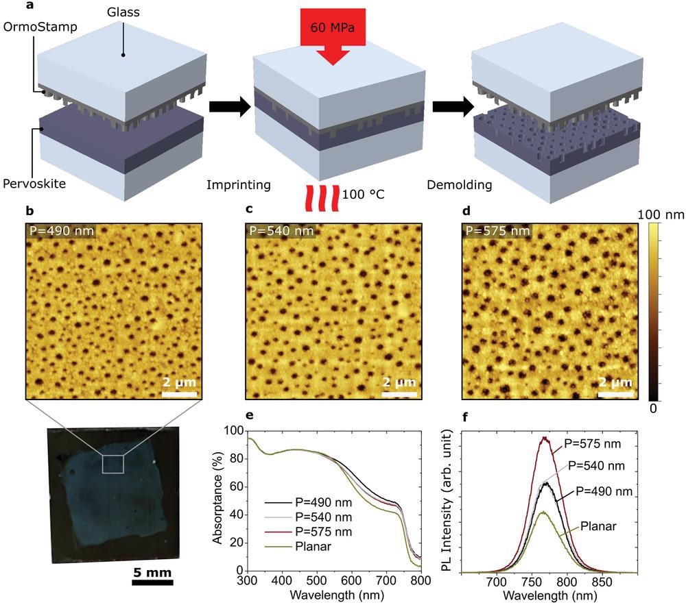
Improved light management in nano-imprinted perovskite films using PSN based imprinting stamp. a) Schematic illustration of the imprinting process of the perovskite films on glass using P2P NIL tool. Imprinting stamps with surface relief shown in Figures 1d and 3a(iii,iv) are used for the thermal NIL process. The calculated P of the nano-stamps are shown in Table 1. b–d) AFM images of the corresponding nano-imprinted perovskite films with effective period of b) P = 490 nm, c) P = 540 nm, and d) P = 575 nm. The photograph of the imprinted perovskite film using P = 490 nm is shown in (b). e) Optical absorption of the planar and the patterned perovskite films with a thickness of 250 nm. f) PL spectrum of the planar perovskite film compared to the PL spectrum of three different nano-imprinted films. Image Credit: Donie, Y. J., et al
Applications
The developed PSN (made of Ormostamp) has a wide range of application sectors. The versatility of the techniques enables several advancements, including nano-transfer printing - transferring patterns across substrates by changing the adhesive forces between the OrmoStamp and the substrate.
Furthermore, the PSN produced may be used as antimicrobial coats and light regulation nanotechnology in optoelectronic devices. The generated nano-stamps with structural disorder are extremely appealing for designing effective light management patterns for large optoelectronic devices requiring a cost-effective imprinting process. Photovoltaic panels and light-emitting devices are two extremely significant applications.
Continue reading: The Applications of Nanoparticles as Synthetic Catalysts.
Reference
Donie, Y. J., Yuan, Y. A., et al. (2021) A Self-Assembly Method for Tunable and Scalable Nano-Stamps: A Versatile Approach for Imprinting Nanostructures. Advanced Materials Technologies. Available at: https://onlinelibrary.wiley.com/doi/full/10.1002/admt.202101008
Disclaimer: The views expressed here are those of the author expressed in their private capacity and do not necessarily represent the views of AZoM.com Limited T/A AZoNetwork the owner and operator of this website. This disclaimer forms part of the Terms and conditions of use of this website.