Nanotwinned materials have been studied extensively over the last decade following the discovery of their much higher hardness and strength than their twin-free counterparts. Despite the frequent encounter of twinning in nanocrystals during the chemical, mechanical, and thermal processes, their nucleation and propagation mechanisms remain elusive.

Study: Swap motion–directed twinning of nanocrystals. Image Credit: Yurchanka Siarhei/Shutterstock.com
An article published in Science Advances demonstrated twinning in the lead (Pb) individual nanocrystals by utilizing in situ atomic resolution transmission electron microscopy (TEM). The results revealed that twinning occurred due to the shift of atomic layers relative to one another through a double-layer swap motion. The swap motion-induced twin nucleation was the crucial step in twin propagation.
The density functional theory (DFT) calculations revealed that the swap motion was the phonon eigenmode of Pb with its face-centered cubic (FCC) crystal structure, which amplified owing to the quantum size effect of the nanocrystals according to theoretical simulations.
Twinning of Nanocrystals
Twinning is a fundamental deformation mode that competes with dislocation slip in crystalline materials. Under high tension, twinning was preferable for dislocation sliding. Deformation twinning has been well documented in FCC nanocrystals.
Twinning occurs in materials in response to heating, laser shock, mechanical stress, electron-beam density, and other external stimuli. Previous studies have reported that twin-structured nanocrystals exhibit greater mechanical strength, increased thermal stability, high electrical conductivity, outstanding light emission, and improved catalytic activity compared to their single counterparts.
Hence, structural modulation of nanomaterials with preferred characteristics is made possible by understanding the transformation twinning mechanisms in nanocrystals. Conventionally, transformation twinning occurs via layer-by-layer partial dislocations in the adjacent atomic planes.
Among external stimulus-induced twinning, only mechanical loading-induced twinning is well-documented. Under external mechanical strain, unusual processes such as synchronous partial dislocation activation, random partial dislocation activation, and a shuffling mechanism are involved in deformation twinning.
Although the conventional deformation twinning mechanism was hypothesized to carry out transformation twinning of nanocrystals, it lacked concrete support. Moreover, external energy is required to break the energy barrier during twinning.
Twin creation in nanocrystals can occur by injecting external energy during thermal annealing or ion or electron irradiation, suggesting that the transformation twinning of the nanocrystals may display unusual paths under the influence of kinetics. Technically, it is challenging to realize twinning excitation and atomic imaging simultaneously because of the speed of partial slip or dislocation, which is assumed to occur as rapidly as the speed of sound.
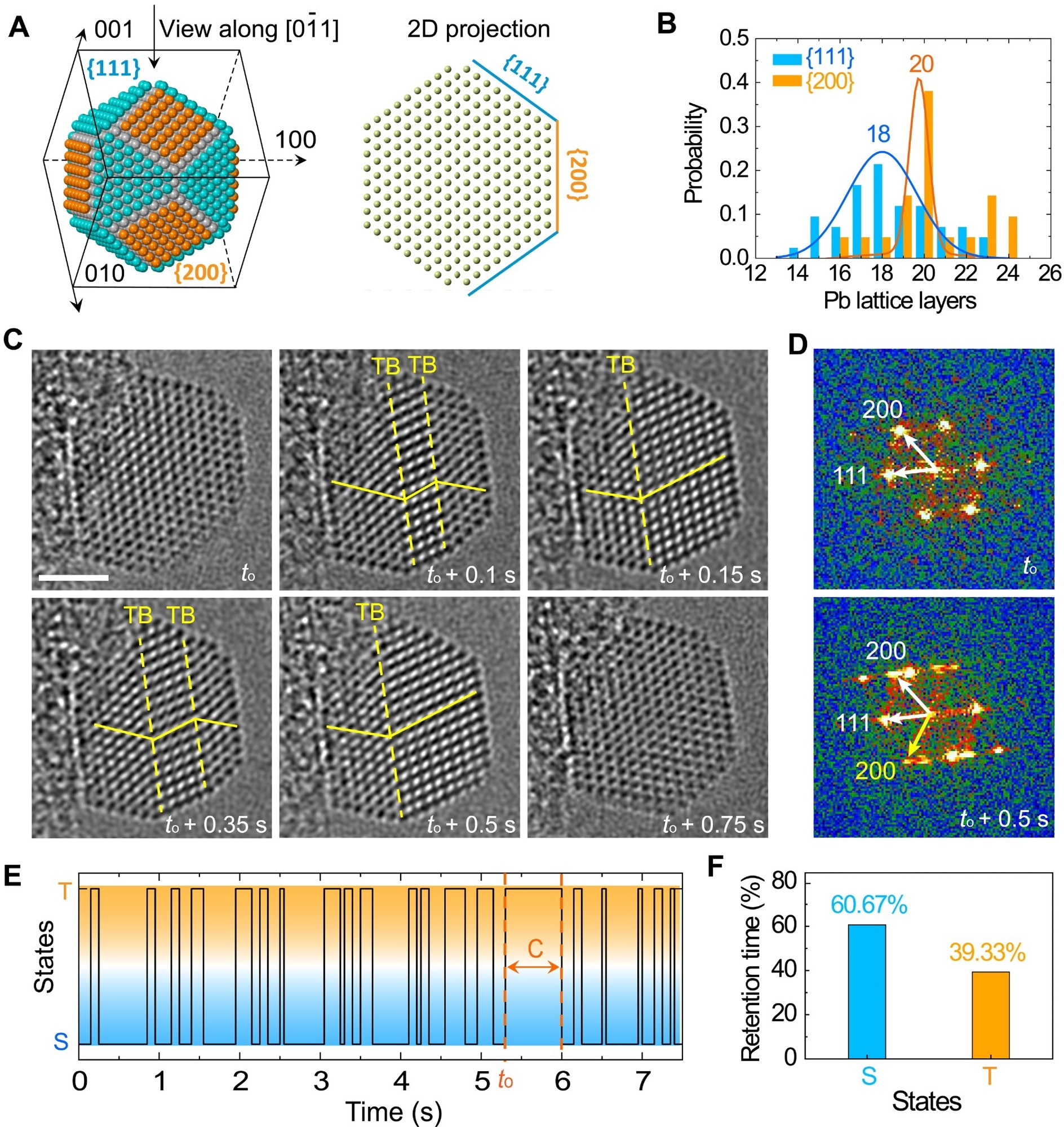
Direct observation of the structural fluctuation between single-crystal and twinned structures of a Pb nanocrystal. (A) Reconstructed 3D atomic model of a truncated Pb nanocrystal and a two-dimensional (2D) projection along the [011¯] showing the view zone axis composed of four {111} and two {200} planes. (B) Histograms of the number of Pb layers along ⟨111⟩ and ⟨200⟩ directions as obtained from the analysis of 36 nanocrystals. (C) Sequential images extracted from movie S3 show the structural fluctuation between the single-crystal (“S”) and twinned structures (“T”) of an individual Pb nanocrystal. TB, twin boundary. Scale bar, 2 nm. (D) Corresponding FFT of nanostructures confirms the single-crystal and twin-crystal structural transformation. (E) Trajectories of structural transitions between single-crystal and nanotwin states during the twinning and detwinning process. (F) The retention time of single-crystal and nanotwin states in movie S3. © Zhang, Q et al. (2022).
Analyzing Twinning of Nanocrystals Via Experimental and Theoretical Studies
Previously, researchers confirmed the superiority of Pb nanocrystals over other materials because of their low melting point and resistance to oxidation, making them ideal candidates for studying structural changes with regulated electron beam irradiation.
In this study, the research team focused on transformation twinning in individual Pb nanocrystals with an FCC crystal structure by employing in situ atomic-resolution TEM with millisecond temporal resolution. Two sophisticated aberrations corrected TEMs were equipped with a high-speed Thermo Fisher Scientific Ceta camera at 40 frames per second and a Gatan K2 IS camera at 400 frames per second to achieve a high temporal resolution.
In situ imaging revealed electron-beam-induced structural transformations in the Pb nanocrystals. The structural fluctuations between the twinned and single nanocrystals were tuned by varying the intensity of the electron beam and the corresponding temperature, demonstrating the impact of electron beam current density on the formation of twin nanocrystals.
On the other hand, subjecting the Pb nanocrystals to an electron beam of the same current density and at cryogenic temperatures did not induce any structural fluctuations, suggesting that transformation twinning was generated by electron beam-induced thermal vibration.
Previous reports have mentioned that nanocrystals dissipate extra energy by phonon vibrations, leading to reversible transformations between twinned and single nanocrystals. Moreover, the retention time of a single nanocrystal is higher than that of its twinned counterpart. Hence, the single-crystal structure lasts longer.
In addition, the transformation dynamics of Pb nanocrystals were theoretically studied using DFT-based phonon calculations, which indicated that the enhancement in the swap mode of the nanocrystals was due to the decrease in the nanocrystal size.
The swap phonon has the lowest energy of all short-wave phonons, making the swap mode the most likely motion mode to occur. As a result, damping may cause a swap model phonon to become a twin. Finally, the experimental findings were observed to be in concurrence with the DFT calculations.
Conclusion
In conclusion, this research demonstrated that the swap motion of two neighboring atomic layers moving regarding one another caused the transformation twinning of Pb nanocrystals. Twin nucleation and twin propagation in the nanocrystals were caused by swap motion. The discoveries of the present study on previously unknown twinning mechanisms offered a new potential for designing and manufacturing nanoscale materials.
Reference
Zhang, Q et al. (2022). Swap motion–directed twinning of nanocrystals. Science Advances. https://www.science.org/doi/10.1126/sciadv.abp9970
Disclaimer: The views expressed here are those of the author expressed in their private capacity and do not necessarily represent the views of AZoM.com Limited T/A AZoNetwork the owner and operator of this website. This disclaimer forms part of the Terms and conditions of use of this website.