Copper (Cu) has applications in the printed circuit board (PCB) industry due to its low electrical resistivity, high electromigration resistance, and good mechanical, chemical, and thermodynamic characteristics.
Part of the PCB process normally involves deposition of Cu by electroplating. Self-annealing is a phenomenon that frequently occurs in electroplated Cu during processing, a concern since it can dramatically alter the structure in terms of grain size, distribution of impurities, and the resulting properties.
In this article, combined with electron backscatter diffraction (EBSD) measurement, KLA Instruments used a high-speed indentation technique to generate the mechanical property maps of the self-annealed Cu.
Materials and Methods
A copper plate coated with a 0.35 µm-thick Cu film used in the printed circuit board (PCB) industry, was used as a substrate. A 20 µm-thick Cu layer was electrodeposited on this electroless Cu film.
The sample was embedded in epoxy and further polished for indentation testing. A KLA Instruments™ iNano® nanoindenter, configured with a Berkovich tip, was used to perform the indentations. NanoBlitz 3D was used to quickly specify an array of 50 x 50 indents within a 50 µm x 50 µm area, with 1 µm spacing between successive indents. The testing time required to perform these 2500 indents was about 40 seconds. The test-control parameters are summarized in Table 1.
Table 1. Summary of test parameters for NanoBlitz 3D on Electroplated Cu. Source: KLA Instruments™
| Input |
Value |
Units |
| Poisson’s Ratio |
0.22 |
None |
| Target Load |
0.32 |
mN |
| X Length |
50 |
µm |
| X Points |
50 |
Integer |
| Y Length |
50 |
µm |
| Y Points |
50 |
Integer |
| Feature Height |
0 |
Nm |
| Target Decrement |
1 |
None |
KLA Instruments gratefully acknowledges Yuan Ze University for providing the Cu pillar samples.
Results and Discussion
The crystallographic evolution of electroplated Cu was identified and mapped with EBSD using field-emission scanning electron microscopy (SEM), as shown in Figure 1, where color represents the crystallographic orientation. Figure 1a shows a the random distribution of the Cu crystallographic orientation, where the Cu grain growth was observed in certain areas of the Cu pillar.
Nanoindentation tests were performed over the same area using the NanoBlitz 3D high-speed mapping option. The hardness maps (Figures 1c and 1e) reveal significant differences between the nanograin regions and the micrograin regions. Larger-grain-size regions (Figures 1d and 1e) show lower hardness values, complying with the inverse relationship between grain size and yield strength (hardness) as proven by the Hall-Petch equation.
The combination of these two analyses, using EBSD and NanoBlitz 3D techniques, can provide a comprehensive characterization of the structure-property relationship in electroplated Cu films.
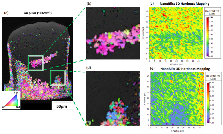
Figure 1. (a) EBSD orientation maps of the electroplated Cu with j=10 A/dm2; (b, d) zoomed-in EBSD maps; (c, e) hardness mapping using NanoBlitz 3D. Image Credit: KLA Instruments™
Summary
High-speed nanoindentation using NanoBlitz 3D was used to map the local hardness of an electroplated Cu. Testing is fast and automated, capable of generating vast amounts of data, thus providing better statistics. The measurements are local, thus revealing important spatial variations in properties.

This information has been sourced, reviewed, and adapted from materials provided by KLA Instruments™.
For more information on this source, please visit KLA Instruments™.