The NanoWizard® V integrates high spatio-temporal resolution with a large scan area, adaptable experiment design, and excellent integration with the latest optical microscope systems. The alignment, automated setup, and re-adjustment of system parameters set the stage for new possibilities for long-lasting and self-regulating experiments series.
Benefits
Automation
Perfecting performance, increasing productivity
Automated workflow, setup, and calibration offer new possibilities for long-lasting, self-regulating experiment series and complicated experimental routines.
Dynamics
Real-time visualization
Analysis of dynamic processes such as growth, crystallization, melting, and domain building at 400 lines/second.
Large samples
Fast scanning over a large scan area
Ground-breaking fast scanning abilities on rough surfaces and samples varying from polymers to solar cells.
Discover the Fifth-Generation Nanowizard Nanoscience AFM
Nanowizard® V sets a new benchmark in automation while offering a multitude of new technical abilities.
Features include:
- New generation packed with novel innovations
- Proven legacy of success via an install base of almost 1000 JPK/Bruker nanowizard AFMs worldwide
- Unmatched ease-of-use
- Perfect for multi-user imaging facilities
- Aided by devoted cantilever development for fast scanning, high-resolution imaging, and tailored applications
- Intuitive V8 software platform
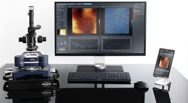
Image Credit: Bruker Nano GmbH - JPK BioAFM
Perfected Performance and Increased Productivity
The NanoWizard V is an excellent nanoscience tool, integrating technical innovation with performance and user comfort.
Setting the stage for new scientific discoveries:
- Lowest noise scanner and detection system guarantees high-resolution data and peerless performance
- Automation for improved productivity and maximized throughput
- Perfect for real-time investigation of dynamics
- High-speed scanning rates ranging up to 400 lines/seconds
- DirectOverlay for AFM in combination with improved optical microscopy
- Features the new Experiment Planner and Experiment Control options
- High-resolution nanomechanical imaging together with the PeakForce-QI™, PeakForce Tapping®, PeakForce QNM, and QI
- Extensive range of accessories available for electrical measurements, environment control, and more
Topography image of atomic lattice of mica in liquid. Image taken in closed-loop TappingMode operation on an inverted microscope. Scan size: 10 nm × 10 nm, height range: 220 pm. Image Credit: Bruker Nano GmbH - JPK BioAFM
Superior Performance
- Imaging from atomic lattices to large-scale samples is versatile
- Highest range of add-ons
- Improved storage of parameters and favorite settings
- Users can capture quick dynamic processes in tough surroundings
- Intuitive user operation available
- Expanded optical viewing field available for AFM with a tiling feature
- Standardized batch analysis routines can be performed for the generation of statistically applicable datasets
- Completely automated cantilever and detector alignment
- Follow reactions throughout several time scales, from milliseconds to seconds and minutes
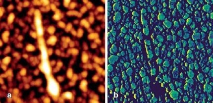
Topography image of hexacontane (C60H122) deposited on highly oriented pyrolytic graphite (HOPG). The image was taken in TappingMode under ambient conditions. Several monomolecular layers of hexacontane are observed. The hexacontane molecules form visible lamellar stripes within each layer. Scan size: 400 nm × 400 nm, height range: 1.04 nm. Image Credit: Bruker Nano GmbH - JPK BioAFM
The performance of NanoWizard AFMs is exceptional. In the NanoWizard V, Bruker have built on this with automated alignment and fast imaging even at large scan sizes, solving real user problems. This instrument will expand the range of experiments possible and make what were once difficult experiments routine.
Dr Nic Mullin, Senior Experimental Officer, Biophysical Imaging Center, Department of Physics and Astronomy, Sheffield

Image Credit: Bruker Nano GmbH - JPK BioAFM
Comprehensive Nanomechanical Characterization
Bruker constantly strives to enhance the nanomechanical characterization abilities of its AFMs and to offer simple technology solutions for complicated scientific endeavors.
The NanoWizard V is the perfect solution for measuring nanomechanical properties and comprehending their vital role in morphology, structure, and molecular interactions.
The NanoWizard V forces the boundaries of science, setting the stage for the AFM technology to an extensive range of applications and making nanomechanical characterization quicker, simpler, and highly accessible for users of all fields of science.
PeakForce-QNM image of a thin film of styrene-ethylene-butylene- styrene triblock copolymer (Kraton G1652) prepared on a silicon wafer. The topography is shown at the top and the corresponding Young’s modulus is shown below. Scan size: 1 µm × 1 µm. a) Height range: 22 nm; b) Modulus range: 280 MPa. Image Credit: Bruker Nano GmbH - JPK BioAFM
Unrivaled Capabilities
- Rapid scanning and user-friendliness integrated with nanomechanical and topographic imaging
- Intuitive and powerful RampDesigner software is available
- True and real-time force curve monitoring
- Characterization of viscoelastic properties with the help of microrheological measurements
- Comes with contact resonance for mechanical characterization of stiff samples (>10 GPa)
- Mechanical mapping integrated with electrical sample characterization in a single run
- Highly sensitive force control and tip-saving features
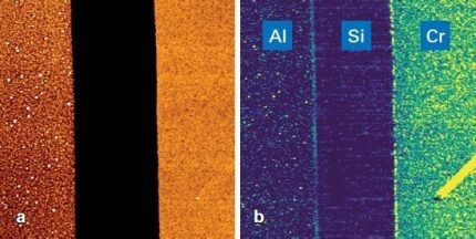
Contact resonance measurement on a layered sample consisting of aluminum, silicon and chromium. Scan size: 12 µm × 12 µm. a) Height range: 121 nm; b) Modulus range: 107 GPa. Image Credit: Bruker Nano GmbH - JPK BioAFM
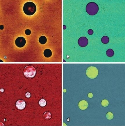
PeakForce QNM image of a blend of polystyrene (PS) and ethylene-octene copolymer. The softer ethylene-octene copolymer (~0.1 GPa) is embedded in a stiff matrix of PS (~2 GPa). Scan size: 4 µm × 4 µm. a) Height range: 80 nm; b) Adhesion range: 10 nN; c) Deformation range: 50 nm; d) Modulus range: 3 GPa. Image Credit: Bruker Nano GmbH - JPK BioAFM
New Chapter in Quantitative Imaging
PeakForce-QI, the symbiosis of PeakForce Tapping and QI mode, delivers unique quantitative nanomechanical imaging capabilities.
It combines the highest acquisition rates with advanced force control to deliver high-resolution, multi-parametric images. The availability of automated setup, operation, and calibration makes it simple to configure and run an experiment and quickly achieve top-quality images and data, even for non-experts.
Powerful Data Analysis
- Adaptable production of topography images at various forces
- Simple and trustworthy batch processing
- Zero force (contact point) imaging. Users can image stack output of any channel from batch processing
Automation and Intuitive Operation at Its Best
The NanoWizard V has been developed to fulfill specific requirements in research and industry. Innovative hardware and software solutions have resulted in increased throughput, automated measurement procedures, and batch processing routines that enable researchers to concentrate on what is essential for their study.
Highest Level of Automation
- Instinctive scripting of automated experiments along with ExperimentPlanner
- It is possible for automated cantilever calibration
- Automated alignment of the laser detection system
- Automated multi-region imaging with the help of motorized stage or HybridStage
- ExperimentControl available for remote tracking of experiments
Intuitive Operation
- Workflow-based software with basic user-friendly features
- Extensive data processing routines can be performed
- An integrated camera can be used for laser detection system alignment
- User management, perfect for multi-user facilities
- Convenient saving of parameters and favorite settings
- Combined software assistance
- Single-click optical image calibration
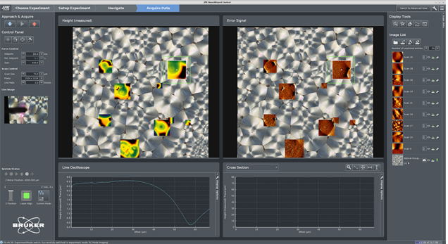
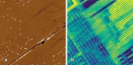
Software setup Latest workflow-based SPM Control Software V8 depicting DirectOverlay 2, DirectTiling, and MultiScan features. Image Credit: Bruker Nano GmbH - JPK BioAFM
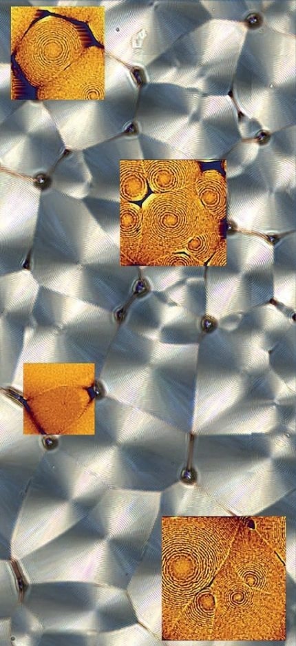
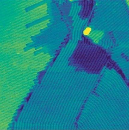
Superposition of optical images from an inverted optical microscope with AFM scans on a thin film of crystallized Poly(3-hydroxy-butyrate-co-3-hydroxyvaler-ate) (PHB/V). The background optical image was created by tiling a series of smaller images (4 × 4 images) using a motorized stage. Crossed polarizers were used to visualize the spherulitic structure of the sample. AFM phase images were acquired in TappingMode under ambient conditions. The periodic, ring-like structures seen in the AFM scans result from the continuous twisting of the crystalline lamellae, forming so-called banded spherulites. Scan size from top to bottom: 50 µm × 50 µm, 60 µm × 60 µm, 45 µm × 45 µm, 70 µm × 70 µm. Image Credit: Bruker Nano GmbH - JPK BioAFM
Unrivaled Flexibility by Design
The renowned tip-scanner technology and modular design of the NanoWizard V NanoScience AFM can be smoothly combined with advanced optical methods.
An extensive range of advanced modes and accessories make it a highly flexible AFM that provides versatility for experimental setups and environmental control.
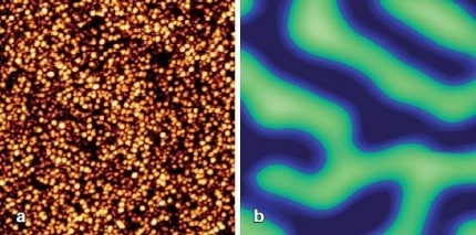
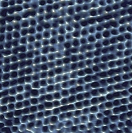
Magnetic force microscopy (MFM) on meander domains with perpendicular magnetization of a multilayer Co-Pt film on silicon. Sample courtesy Dr V. Neu (Leibnitz IFW Dresden, Germany). Scan size: 1µm × 1µm. a) Height range: 4 nm; b) Phase range: 14.4 deg. Image Credit: Bruker Nano GmbH - JPK BioAFM
Comprehensive range of add-ons and accessories
- Extensive range of temperature control accessories (–120 °C up to 300 °C)
- Scanning Thermal Microscopy (SThM)
- Magnetic Force Microscopy (MFM)
- Comes with stretching stages
- Several fluids cells
- Nanomanipulation is provided
- Friction force microscopy
- Multimodal imaging can be performed
Kelvin Probe Force Microscopy (KPFM, dual-pass) on a DRAM (Core 2 Quad processor, Intel). Scan size: 85 μm × 85 μm. a) Height range: 68 nm; b) CPD range: 468 mV. Image Credit: Bruker Nano GmbH - JPK BioAFM
High-resolution electrical characterization
- Conductive AFM (CAFM)
- Kelvin Probe Force Microscopy (KPFM)
- Scanning Tunneling Microscopy (STM)
- Scanning Electrochemical Microscopy (SECM)
- Electrostatic Force Microscopy (EFM)
- Piezo Force Microscopy (PFM)
For complex experiments, from polymers to solar cells
- Improved environmental control options
- Several modes for long-lasting and neglected experiments
- Optical accessibility of the sample, for example, for specified illumination
- Detection laser option ranges to 980 nm
Conductive AFM (CAFM) of zinc oxide deposited on niobium-doped strontium titanate (bias voltage -4.0 V). Sample courtesy Prof. F. Bobba, University of Salerno, Italy. Scan size: 850 nm × 850 nm. a) Height range: 16 nm; b) Current range: 42 nA. Image Credit: Bruker Nano GmbH - JPK BioAFM
Piezoresponse Force Microscopy (PFM) of a ferroelectric polymer P(VDF-TrFE) on a gold back electrode on silicon. A sequence of voltage pulses (20 V) was generated from a bitmap template to write the logo into the piezoelectric polarization of the sample. Vertical PFM-phase image after patterning is shown. Scan size: 45 µm × 10 µm Phase range: 170 deg. Image Credit: Bruker Nano GmbH - JPK BioAFM
![SECM scan of a platinum electrode on glass taken in force mapping mode. The topography image is overlaid with a vertical section through the recorded SECM current distance dependence (tip potential -0.3 V, electrode potential 0 V, 10 mM [Ru(NH3)6]3+ in 0.1 M KCl). The expected behavior of redox-cycling (on electrode) and blocking (on glass) is clearly observed. Scan size: 15 μm × 10 μm Current range: 200 pA.](https://www.azonano.com/images/equipments/EquipmentImage_2036_16693668466407494.jpg)
SECM scan of a platinum electrode on glass taken in force mapping mode. The topography image is overlaid with a vertical section through the recorded SECM current distance dependence (tip potential -0.3 V, electrode potential 0 V, 10 mM [Ru(NH3)6]3+ in 0.1 M KCl). The expected behavior of redox-cycling (on electrode) and blocking (on glass) is clearly observed. Scan size: 15 μm × 10 μm Current range: 200 pA. Image Credit: Bruker Nano GmbH - JPK BioAFM
The New Benchmark for Fast Scanning of Large Samples
The NanoWizard V NanoScience platform provides quick scanning over a large scan area. The complete scan range in all three axes remains accessible, offering peerless scanning speeds and simple switching between sample features. This can be done in the absence of sample relocation or a decrease in imaging speed.
The Fast-Scanning option is perfect for analyzing dynamic processes, offering the speed and precision essential to study phenomena, such as growth, melting, crystallization, and domain building, in real-time.
Innovative fast scanning capabilities in an automated AFM
- Enhanced productivity and improved throughput for trustworthy statistics
- Fast z-piezo with high resonance frequency offers quickest feedback
- Active balancing enables quick scanning over large scan areas
- NestedScanner technology offers quick scanning of corrugated samples with a z-range of up to 16.5 µm
- Adaptive intelligence-based scanning routines allow scanning rates of up to 400 lines/seconds
High-resolution electrical characterization
- Conductive AFM (CAFM)
- Electrostatic Force Microscopy (EFM)
- Scanning Tunneling Microscopy (STM)
- Piezo Force Microscopy (PFM)
- Scanning Electrochemical Microscopy (SECM)
- Kelvin Probe Force Microscopy (KPFM)
Stability and highest data accuracy meet ease-of-use
- Movie creator
- Quick scanning with sophisticated closed-loop control
- Fast z-piezo fitted with capacitive sensor for greatest data precision
- DirectDrive feature available for high cantilever excitation stability
- Precise force control as a result of the new feedback technologies
- Batch processing and advanced data analysis routines
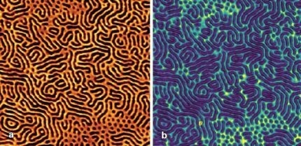
Representative series of phase images taken in TappingMode on a thin film of Poly(3-hydroxybutyrate-co-3-hydroxyvalerate) (PHB/V). Prior to the measurements, the sample was heated to above the melting temperature and then cooled to below the melting temperature immediately before image acquisition. The images show a growth front of the crystallizing PHB/V passing through the scan area. The time difference between each of the displayed images is 18 seconds. The actual data acquisition was running at 2.5 seconds per frame. Scan size: 600 nm × 600 nm Pixel size: 512 px × 512 px Scan speed: 200 lines/sec Phase range: 20 deg. Image Credit: Bruker Nano GmbH - JPK BioAFM
Applications
NanoWizard NanoScience Data Gallery
Bruker’s BioAFMs enable life science and biophysics scientists to add to their investigations in mechanobiology, cell mechanics and adhesion, cell dynamics, cell-cell, cell-surface interactions, and cell morphology.