Vistec Electron Beam GmbH, a global leader in electron-beam (e-beam) lithography systems, will present its latest advancements in e-beam technology at the 41st European Mask and Lithography Conference (EMLC 2026), taking place June 22-24, 2026, at the Volkshaus in Jena, Germany. This year also marks a significant milestone for Vistec, celebrating 30 years as a company, built upon more than 60 years of e-beam technology expertise. Over the past year, Vistec has achieved several key developments, including new customer installations, expanded global presence, and continued innovation in its core lithography technologies. The company’s participation at EMLC highlights its innovative developments enabling advanced semiconductors, photonics, micro-optics, biosensing MEMS/NEMS, and quantum computing for both industrial and advanced research applications.
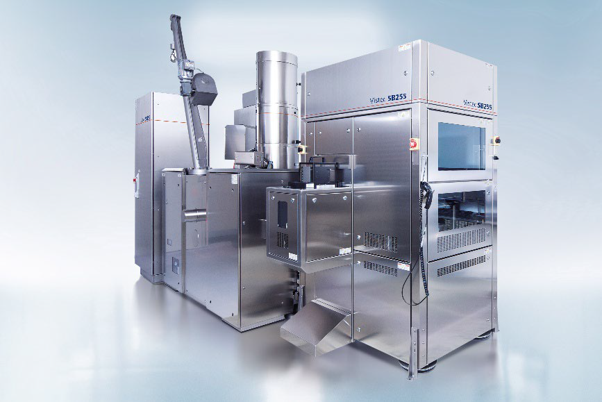 The Vistec SB255 e-beam system is a high-resolution, universal and cost-effective tool supporting both direct write and mask-making applications. Image Credit: Vistec Electron Beam GmbH
Advanced Electron-Beam Lithography
The company’s e-beam lithography systems are based on Vistec’s proprietary Variable Shaped Beam (VSB) technology, which enables high-precision patterning with superior flexibility. Unlike traditional Gaussian beam systems, which expose features point-by-point, VSB technology writes variable-sized shapes, which range from nanometer- to micron-scale, to significantly reduce shot count and improve write time. When combined with advanced Cell Projection, which enables repeated and even arbitrary structures to be exposed in a single exposure step, Vistec systems deliver substantial throughput gains for applications with recurring geometries such as photonics, micro-optics and AR/VR waveguides.
Vistec’s VSB platforms provide a cost-effective, flexible e-beam lithography solution that maintains high resolution and pattern fidelity while supporting a broader range of applications, particularly in high-mix/low-volume production environments. The company’s platforms also support 300-mm wafer writing, positioning them for both advanced research and industrial manufacturing. Another key differentiator is Vistec’s proprietary ePLACE data preparation software, which streamlines data processing workflows and optimizes exposure strategies, including Cell Projection, for its VSB systems.
New Customer Engagements and Milestones
In Japan, Vistec recently completed the installation of an SB255 VSB system in the Takeda Sentanchi Super Cleanroom at The University of Tokyo (UTokyo) as part of the Advanced Research Infrastructure for Materials and Nanotechnology - Semiconductor Technology Infrastructure Initiative (ARIM-SETI). The Takeda Sentanchi Super Cleanroom is operated by Platform Device Research Division, Systems Design Lab (d.lab), Graduate School of Engineering, UTokyo. A high-resolution, universal and cost-effective tool supporting both direct write and mask making applications, the Vistec SB255 enables UTokyo to gain broader access to advanced applications. In addition, this installation represents a significant step in growing Vistec’s presence in the strategically important Japanese market. UTokyo partners with both Vistec, a member of the HEIDENHAIN Corporate Group, and HEIDENHAIN K.K. (Japan) as key industry suppliers to support precision research, materials science, and semiconductor lithography education.
In addition, Vistec has seen strong adoption across compound semiconductor foundries, with a double-digit number of system installations supporting advanced device manufacturing. In the United States, Vistec will supply an e-beam lithography system to a major technology innovator for an advanced research project, further highlighting the expanding role of e-beam technology in next-generation device innovation. Additional customer engagements in Europe further reflect growing demand for flexible, high-resolution lithography solutions.
In Taiwan, Vistec has maintained a strong regional presence for more than 20 years, supported by its local subsidiary, Vistec Electron Technology Co. Ltd., which provides dedicated field service engineering support to customers throughout the region. The company also works closely with its sales representative, Scientech Corporation, to support customer engagement and business development across the Taiwanese market. Vistec continues to expand its footprint with the ongoing installation of a 300-mm e-beam lithography system at the Taiwan Semiconductor Research Institute (TSRI), operating under the National Institutes of Applied Research (NIAR), following the successful installation of a
200-mm system last year. Vistec also serves customers in Taiwan’s compound semiconductor foundry market.
“With a heritage spanning more than 60 years, we continue to build on our reputation as an e-beam expert, delivering solutions that bridge advanced research and industrial-scale applications,” said Matthias Slodowski, General Manager at Vistec Electron Beam GmbH. “Driven by increasing demand for photonics, advanced semiconductor devices, and specialized manufacturing processes, the need for flexible, high-precision lithography solutions continues to grow. Our world-class VSB lithography platforms with seamless integrated Cell Projection technology provide the enhanced throughput, precision, flexibility, high automation and manufacturing efficiency to meet these needs. Today, e-beam technology is a critical enabler of future innovation for tomorrow’s advanced devices, and we are excited to showcase our latest technology advancements and application expertise at EMLC 2026.”
Presentations at EMLC 2026
Vistec is participating in the EMLC program with the following talks:
- “E-beam Cell Projection for 3D Blazed Gratings and Curvilinear Features” (Session 4: Wafer Lithography and Patterning, Monday, June 22, 17:20-17:40)
- “Role of Shape Approximation in Determining Waveguide Properties Using Variable-shaped E-beam Lithography” (Session 4: Wafer Lithography and Patterning, Monday, June 22, 17:40-18:00) – co-authored with Fraunhofer Institute for Applied Optics and Precision Engineering, Friedrich Schiller University and Max Planck School of Photonics
- “Stacked Grayscale Lithography Using Intra-level E-beam Exposure on Latent Resist Image of i-line Structures Using Specialized Data Preparation Methods” (Session 10: Novel Lithographic Technologies / Direct Write Lithography and Patterning, Poster Presentations, P-3, Tuesday, June 23, 16:30 to 18:20) – co-authored with Fraunhofer Institute for Electronic Nano Systems and Technische Universität Chemnitz (the Chemnitz University of Technology)
Attendees at EMLC 2026 are invited to connect with Vistec to learn more about its latest technology developments. Contact Ines Stolberg, Manager Marketing & Sales at: [email protected].