In this article, the most common errors occurring at different stages of the semiconductor fabrication process and the strategies to mitigate them are discussed.
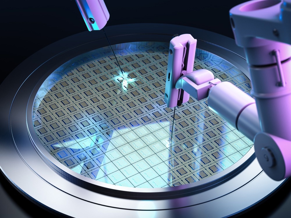
Image Credit: Phonlamai Photo/Shutterstock.com
The ever-growing complexity of the semiconductor manufacturing process, mainly due to the introduction of new technological nodes and the increasing transistor packing density, demands more sophisticated equipment and elaborated methods.
Despite advances in semiconductor manufacturing technology, fabrication and testing errors are still an indispensable part of semiconductor manufacturing.
Almost every sector of modern electronics relies on using a wide variety of semiconductor devices. From mobile phones and laptops, through microwaves and fridges, to solar panels and LED displays, all these gadgets and appliances operate using integrated circuits assembled from semiconductor diodes and transistors.
Critical Steps in the Semiconductor Manufacturing Process
The semiconductor manufacturing process involves several stages, including wafer fabrication, assembly, packaging, and final integrated circuit testing.
Wafer fabrication can be divided into several sub-processes, such as photolithographic patterning, etching, and doping of the wafer, and metal or semiconductor layer deposition, to define the desired electrical properties of the semiconductor components. The individual components are then transferred onto a substrate and assembled into a functional integrated circuit. Finally, the functionality of each semiconductor component and the assembled circuit is tested to pinpoint and rectify any manufacturing defects.
Most of the semiconductor manufacturing steps are automated and performed in an ultraclean environment with a high level of quality control to minimize manufacturing errors and defects. Despite that, fabrication errors can still occur at different stages of the manufacturing process, causing degradation of the performance and reliability of the semiconductor devices.
Errors Related to the Photolithographic Pattern Transfer
The shrinking dimensions of the semiconductor components, enabled by modern extreme UV light sources, make the semiconductor fabrication process very susceptible to errors occurring during the various photolithographic steps, such as mask alignment, photoresist patterning, and the subsequent pattern transfer (etching).
Photolithographic errors can cause photoresist over- or under-exposure, irregular line width, non-uniform etching, and missing or misaligned features, resulting in semiconductor components with incorrect dimensions and out-of-specification performance.
Process Parameter Fluctuations Causing Electrical Defects
Critical process parameters, such as temperature, pressure, humidity, and timing, are crucial for ensuring the high quality and performance of the semiconductor components. Fluctuations of these parameters can cause wafer contamination with dust or chemical impurities, incorrect doping concentration, non-uniform dopant distribution, incorrect layer thickness, and others. For example, doping errors can alter the electronic levels of the semiconductor bandgap and can lead to the manufacturing of semiconductor components with inadequate electrical properties and short lifetimes.
Human Errors and Equipment Malfunctions
Despite the high level of automation in semiconductor manufacturing, human input and intervention are still required at different stages of the fabrication process, such as initial process setup or handling and testing of the semiconductor devices.
Some of the most common human errors include the input of incorrect parameters, improper setup, failure to detect process anomalies, lack of focus, and others. Human errors can result in misaligned or damaged wafers and inadequate quality control.
In addition to human errors, equipment malfunctions can occur during any step of the semiconductor manufacturing process, resulting in manufacturing yield losses and failures of the final assemblies.
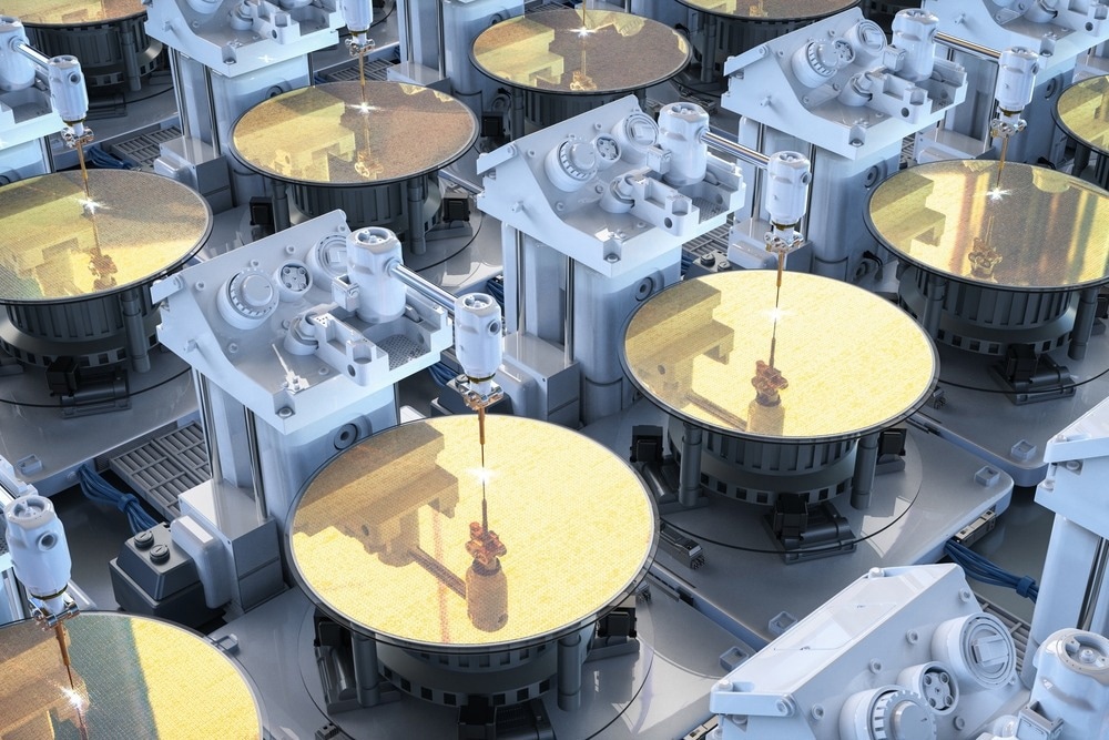
Image Credit: Phonlamai Photo/Shutterstock.com
Strategies to Mitigate Manufacturing Errors
As the semiconductor industry moves towards more advanced lithography techniques, enabling device fabrication at the 10-nm node and beyond, several strategies are being developed to mitigate the manufacturing errors described above.
Simulating Manufacturing Errors
Artificial intelligence-based integrated process control approaches are adopted to monitor their entire supply chain, starting with the source materials, and control each manufacturing process step. Apart from controlling the processing and environmental parameters, these control routines schedule regular equipment maintenance and calibration to ensure the correct functioning of the equipment and minimal downtime of the production lines.
Advanced computer simulation tools enable semiconductor manufacturers to devise and test the entire fabrication process in silico before it is implemented in hardware. This approach helps to identify and correct any potential process errors before setting up a production run.
Automated Real-Time Inspection Tools
Real-time monitoring and inspection using machine vision systems and high-throughput high-resolution automated imaging techniques can detect processing errors and enable rapid correction of the processing parameters in real time.
Rigorous testing and quality control at different stages of the manufacturing process, in particular during the packaging and assembly steps, can help to identify and correct any electrical and connectivity faults.
Besides, fully integrated automated control and inspection systems can reduce or eliminate the dependency on human judgment, memory, and compliance, thus eradicating human errors in the manufacturing process.
In summary, using advanced process control, real-time monitoring and inspection, and artificial intelligence-based error correction algorithms enable semiconductor manufacturers to mitigate manufacturing errors and ensure the high quality and reliability of the semiconductor devices.
References and Further Reading
McCluskey, M. D and Janotti, A. (2020) Defects in Semiconductors. Journal of Applied Physics 127, p. 190401. doi.org/10.1063/5.0012677
Tseng, W. P. (2016) Approaches to defect characterization, mitigation, and reduction. Advances in Chemical Mechanical Planarization (CMP), pp. 433-462. doi.org/10.1016/B978-0-08-100165-3.00017-6
Perez, J. A. S. (2017) Risk minimization through metrology in semiconductor manufacturing. Université de Lyon, Thesis. Available at: https://theses.hal.science/tel-02878704
Disclaimer: The views expressed here are those of the author expressed in their private capacity and do not necessarily represent the views of AZoM.com Limited T/A AZoNetwork the owner and operator of this website. This disclaimer forms part of the Terms and conditions of use of this website.