In this interview, we speak with SkyWater Technology about the current state of the semiconductor industry, how nanotechnology has helped to shape this sector, and their new partnership which aims to increase the accessibility of semiconductor chips for start ups and research groups across the United States.
Please could you introduce yourself and tell us about your current position at SkyWater Technology?
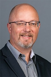
My name is Steve Kosier, and I have the great pleasure of serving as EVP and CTO at SkyWater Technology, the only U.S.-owned pure-play foundry.
I joined SkyWater about a year and a half ago. For most of my career, I worked at Polar Semiconductor and its predecessors and most recently was President of Kanomax FMT, a nanoparticle instrumentation company. All these companies are in the Minneapolis-St. Paul Minnesota metro area.
SkyWater Technology helps actualize innovations for customers; could you discuss the company’s core mission and its services?
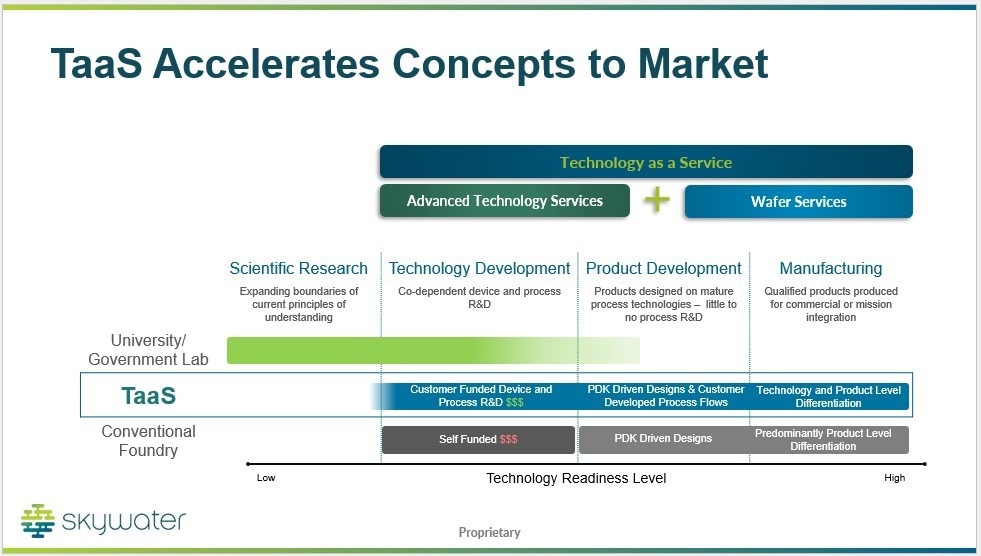
SkyWater’s vision is to improve the world by revolutionizing technology realization. Our business model is the Technology as a ServiceSM (TaaS) model, which means we engage in funded technology development projects in the same facility that we run high-volume production. This allows for a seamless transfer of developed technology into production and is a unique model in our industry.
© SkyWater Technology
Some of your target markets include the aerospace, industrial and automotive sector. What are some of the highlight technologies that you can offer customers in this space?
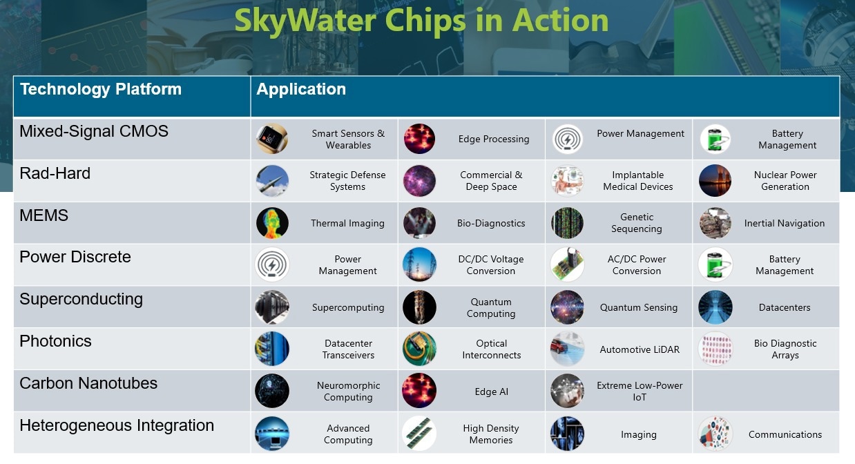
Our main technology in volume production today is mixed-signal CMOS at the 90 nanometer and 130 nanometer technology nodes on 200mm wafers. These wafers end up in many applications and markets, including automotive, consumer, communications, and more.
However, through our TaaS business, we have many capabilities that allow us to engage in Superconducting, Quantum Computing, Silicon Photonics, MEMS, Microfluidics, Power Management, and other areas that require highly differentiated silicon process solutions.
© SkyWater Technology
How do you predict this community to change over the next 30 years? Are there any trends or developments you are looking to monitor?
We think the next era of innovation for this industry involves broadening the reach and usefulness of semiconductors into new applications that are only now emerging. We see how the electronics content in cars continues to grow – all the features that save lives and improve the driving experience are made possible by semiconductors. It is safe to say there will be more, not less, semiconductors in the future.
Some of the megatrends occurring in our industry are the recognition that semiconductors are infrastructure and, as such, represent a vital national resource, much like roads, bridges, electricity, water, and so on. Our foreign competitors have understood this for decades and now the U.S. is taking action to re-shore the complex semiconductor supply chain with the CHIPS + Science Act.
Another major issue for the industry is that semiconductor processing uses tremendous amounts of water, power, and rare earth elements. Some of these elements are found only in certain places worldwide, and these places are becoming more unstable. So, a major geopolitical aspect to semiconductors will become more important in the future.
Finally, the workforce to manufacture semiconductors needs to be trained and developed in the U.S. For instance, Purdue University now offers a Semiconductor Degrees Program to enable a quick ramp-up of skilled talent, creating the next-generation of semiconductor workforce to reassert U.S. prominence in this critical industry.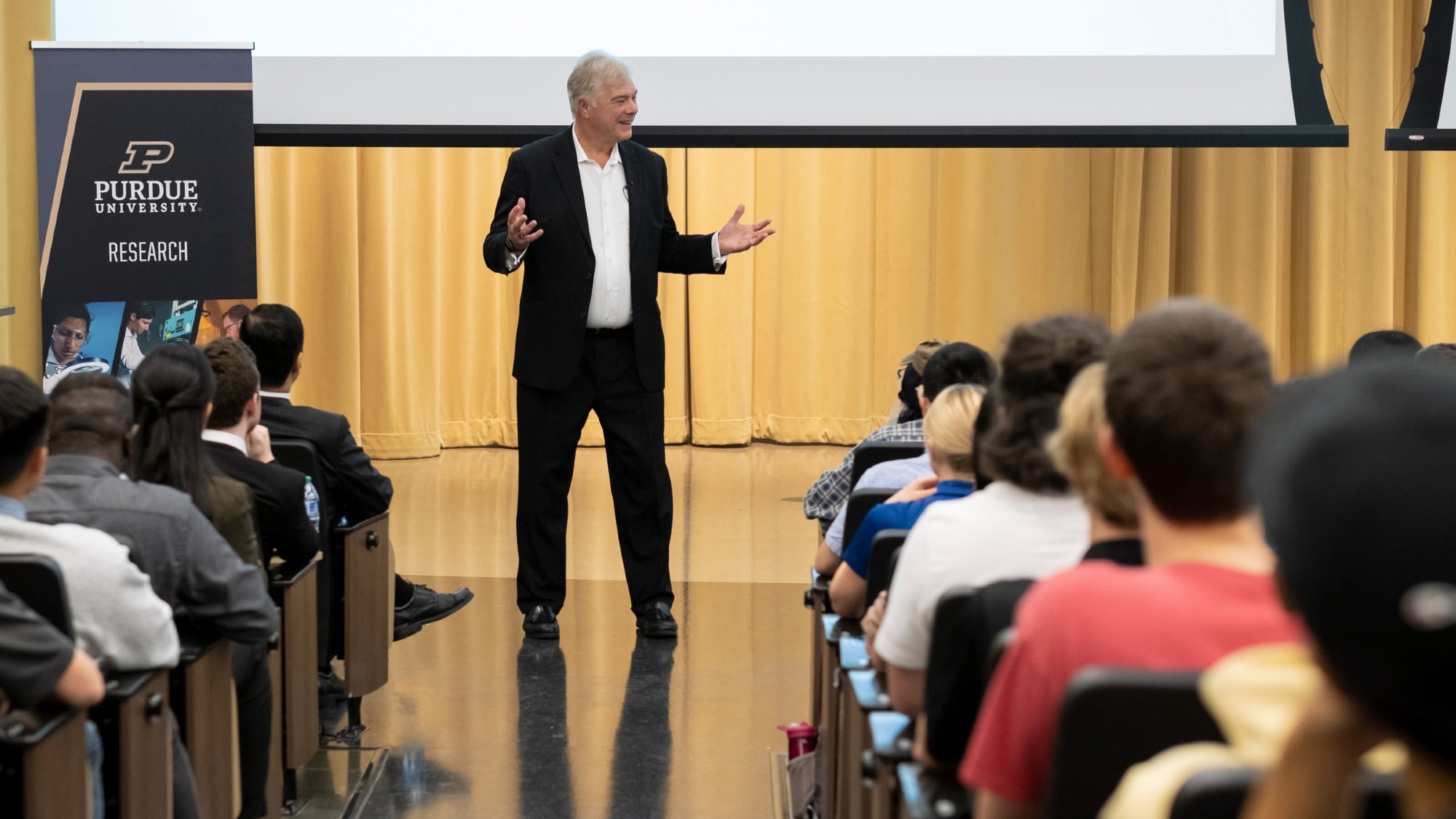
SkyWater’s President and CEO, Thomas Sonderman presents a keynote lecture on 9/13/22 to over 300 engineering students at Purdue, providing real-world scenarios for careers in the semiconductor industry. © SkyWater Technology
A good question to ask the young student who loves writing code is “where do you think that code goes?” - it goes to a physical system somewhere, and microelectronics enable this.
Collaborations across research and industry can help boost innovation and investment across technology and engineering sectors. Could you tell us about your recent partnership with NIST and Google?
Yes, this is exciting for SkyWater and we were pleased that U.S. Secretary of Commerce Gina Raimondo announced this partnership during a visit to Purdue on September 13th.
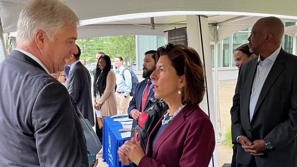
SkyWater President and CEO Thomas Sonderman speaks with U.S. Secretary of Commerce Gina Raimondo at an event at Purdue University on September 13, 2022. © SkyWater Technology
SkyWater, with our partners Google and eFabless, are pioneers in the open-source PDK model. You can go to GitHub, search for SKY130, and download a complete set of design tools and files that allow you to design chips in the 130 nm technology. Through Google-sponsored shuttles, you can even get your chips fabricated for free at SkyWater. The only requirement is that the design must be completely open-source – all the schematics, layouts, files, and so on must be accessible to anyone who wants to view them.
This open-source SKY130 technology base was adopted by NIST, in partnership with Google, to build a nanotechnology accelerator program. This program puts a “lab on a chip” using SKY130, into the hands of researchers. The idea is to process the wafers almost fully and then deliver them to researchers who are conducting interesting experiments on top of the wafers.
Such an approach leverages the scale of multi-project wafers, and the open-source IP community to allow research on a scale that has never been seen before. It’s a great program and we are excited about all the possibilities that will follow.
A driving force behind this collaboration is to improve chip supply to research and start-ups across the U.S. One may ask why it is beneficial to dedicate initiatives to smaller enterprises and what impact this can have on boosting the industrial landscape of a country.
The program is about access. Anybody can learn to program a computer by learning C++, Java, Python, whatever – because all you need to do is get a free compiler and watch some videos and learn on your own – with no NDAs to sign, money to spend, or barriers at all. Chip design is almost the opposite – you need millions of dollars, proprietary tools, college-level courses, signed NDAs, and so on. As a result, very few people will ever design a chip.
Until now.
With the open-source tools that are available, all these barriers are removed, and anybody can design a chip.
We see universities, community colleges, and even high schools designing chips and all sorts of tutorials on YouTube on how to design. Such a movement is transformative, game-changing and brand new to the industry; it is a step towards workforce development, greater awareness, and universal access – truly democratizing chip design.
October 9th marks Nanotechnology Day, which aims to spread awareness about how nanoscience has benefitted our lives. Over the course of your career, how have you seen the nanotechnology community grow, and what impact has it had on the semiconductor industry?
The semiconductor industry has grown in fits and starts over the decades, as the business is inherently cyclical. Some of the latest projections are that it will surpass $1T by 2030. While much of the focus and attention goes towards the technology that makes the most advanced chips using the smallest features (3 nanometers today) and the most expensive factories ($20B to construct such a factory), most of the chips produced and used worldwide are made at less advanced and less expensive technology nodes.
At these nodes, where SkyWater exists, the emphasis is on all the remarkable things that can be done with silicon in new and innovative ways to tailor the process to the application requirements.
What are the next steps for SkyWater Technology?
With the passing of the historic CHIPS & Science Act of 2022, we will continue to co-create solutions with our customers by expanding capacity at our Minnesota facility, continue bringing our Florida fab online and plan for a new $1.8B facility at Purdue.
As we continue to grow and scale our business, we are constantly searching for people who want to be part of the TaaS revolution.
About Steve Kosier, Ph.D.
 Steven Kosier is responsible for the Advanced Technology Services (ATS) business execution within SkyWater, partnering with companies to co-create their innovative process flows from concept to mass production. He is also responsible for forming and managing strategic technology partnerships and alliances, developing the company’s technology roadmap and IP strategy, and growing the value of the company’s technology portfolio.
His background includes 25 years of experience and successive growth in technical, marketing and business leadership positions. A founding member of PolarFab and Polar Semiconductor wafer foundries, he has developed and transferred to volume production many generations of analog, mixed-signal, and high-voltage technologies for automotive and industrial end markets. Most recently, Kosier was president at Kanomax FMT, a nanoparticle measurement instrumentation start-up with industry-leading resolution down to 2 nanometers.
Kosier is an adjunct Professor of Electrical Engineering at Vanderbilt University, where his research interests include radiation effects on microelectronics and semiconductor device reliability physics. He holds 14 U.S. patents and has authored or co-authored more than 30 publications in the areas of radiation effects, high voltage and power devices, integrated magnetic sensors and nanoparticle measurement solutions.
Kosier holds a Bachelor of Science in electrical engineering from the University of Minnesota, and a Master of Science and doctorate in electrical engineering from the University of Arizona.
Disclaimer: The views expressed here are those of the interviewee and do not necessarily represent the views of AZoM.com Limited (T/A) AZoNetwork, the owner and operator of this website. This disclaimer forms part of the Terms and Conditions of use of this website.