Learn about the historical and current materials utilized in semiconductor chips, explore emerging materials proposed as replacements for traditional ones, and examine the challenges associated with current materials.
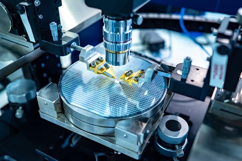
Image Credit: FOTOGRIN/Shutterstock.com
What are Semiconductors?
Semiconductors are materials that exhibit a unique electrical behavior, combining characteristics of both conductors and insulators. At lower temperatures, semiconductors function the same as insulators, obstructing conductivity; however, they transition into a conductive state when exposed to factors like light, heat, or voltage. This unique behavior makes semiconductors integral components in modern electronic devices to control electrical flow.
Semiconductor Chips and Their Components
Semiconductor chips, also known as microchips, are composed of tiny electronic components interconnected through a network of conductive paths etched onto a semiconductor substrate, typically made of silicon, allowing or blocking the flow of electrical current to represent binary information. These semiconductor chips play a crucial role in powering various electronic devices, from smartphones and laptops to complex machinery and industrial equipment.
Materials used in Semiconductor Chips
Historically, silicon has been the central material in semiconductor manufacturing due to its excellent semiconducting properties and abundance in nature. The insulating and conducting layers in traditional semiconductor chips are often made of silicon dioxide and doped silicon, respectively. However, modern chip designs may incorporate various other materials to improve the performance of the chips.
For instance, advanced semiconductor technologies might use high-k dielectrics like hafnium oxide instead of silicon dioxide as an insulating layer. Similarly, metal gates like tungsten or copper have replaced traditional polysilicon gates in certain designs due to their superior conductivity.
Materials in the semiconductor industry that are expected to compete with silicon in the future are two-dimensional materials like graphene and transition metal dichalcogenides (TMDs). Graphene is a 2D material of a single layer of carbon atoms arranged in a hexagonal lattice that exhibits extraordinary electrical conductivity and mechanical strength. Similarly, transition metal dichalcogenides, such as molybdenum disulfide (MoS2) and tungsten diselenide (WSe2), possess unique electronic properties that can be harnessed for semiconductor applications, offering advantages like tunable bandgaps and reduced power consumption.
Recent Developments
Advancements in Semiconductor Wafer Transfer
In a recent study researchers focused on graphene transfer from its growth substrate to another desired substrate since graphene transfer is an integral part of manufacturing graphene-based electronic devices.
The study compared wet and semidry transfer methods for wafer-scale integration, emphasizing factors like scalability, automation potential, yield, contamination, and electrical performance. The wet transfer demonstrated superior yield, lower carbon contamination, and better electrical quality, while semidry transfer exhibited advantages in scalability and automation due to existing industrial tools.
Through this research, the challenges of handling graphene after copper etching in wet transfer were explored, concluding that both methods could benefit from further optimization, with semidry transfer showing potential for applicability and scalability in semiconductor manufacturing.
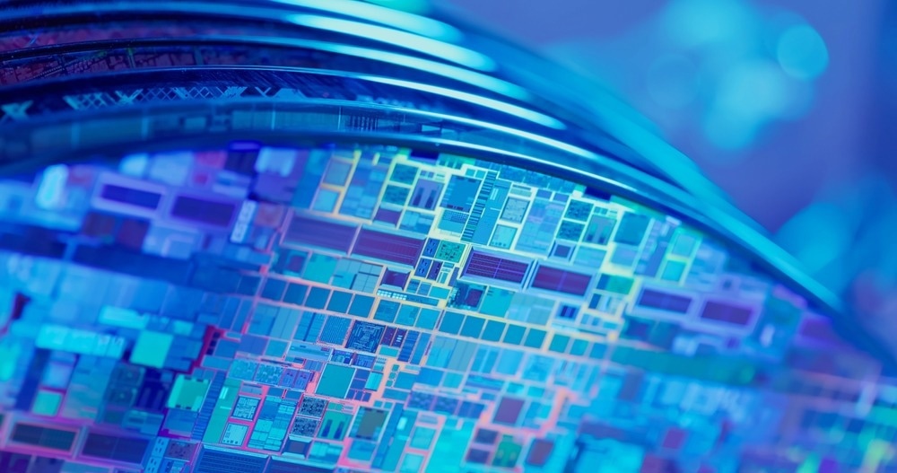
Image Credit: aslysun/Shutterstock.com
Scaling 2D Semiconductor Production
In a 2022 study, researchers addressed the limitations in large-scale production of two-dimensional (2D) transition metal dichalcogenides (TMDs), crucial semiconductor materials for next-gen devices.
Traditionally, TMD wafer production was constrained to small pieces per batch due to challenges in the simultaneous supply of precursors. The study introduces a modularized growth strategy, enabling batch production of 2-inch to record-large 12-inch TMD wafers (15 pieces and 3 pieces per batch, respectively).
Each module facilitates local precursor supply for uniform growth, demonstrating versatility in creating structures like Janus MoSSe, MoS2(1−x)Se2x alloys, and MoS2-MoSe2 in-plane heterostructures. This scalable method aims to transition 2D semiconductor production from lab-scale to industry-scale, providing high-quality wafers for next-gen semiconductor devices beyond silicon technology.
Problems with Current Materials and Blockades to Alternatives
Silicon has been a go-to material in semiconductor manufacturing for a long time. Still, with advancements in technology as the semiconductor industry pushes its limits, the challenges associated with silicon-based semiconductors are becoming evident. For instance, as transistors’ size becomes smaller, leakage currents and heat dissipation issues arise, which leads to reduced efficiency and thermal challenges in high-performance computing.
Transition metal dichalcogenides face challenges related to scalable production and integration into existing semiconductor manufacturing processes. Similarly, despite the exceptional conductivity of graphene, it lacks an inherent bandgap, which is a crucial feature for semiconductor applications. Researchers are exploring ways to induce a bandgap in graphene or combine it with other materials to make it a viable semiconductor.
Conclusion
In conclusion, the semiconductor landscape is undergoing a transformative shift beyond traditional silicon, exploring a diverse array of materials to meet the demands of advancing technology.
From the historical dominance of silicon to the emergence of two-dimensional materials like graphene and transition metal dichalcogenides, the semiconductor industry is at the forefront of innovation.
Recent studies addressing semiconductor wafer transfer and large-scale production challenges demonstrate the ongoing efforts to optimize processes and scale production for these future materials. However, challenges such as the heat dissipation issues with shrinking silicon transistors and the need to induce a bandgap in graphene for practical semiconductor applications need further research to tackle.
References and Further Reading
Ali, Owais. (2023, October 16). The Path to A Sustainable Semiconductor Industry. AZoNano. Retrieved on January 07, 2024 from https://www.azonano.com/article.aspx?ArticleID=6570
Icdrex. (2022) Will graphene replace silicon as a semiconductor material? Industry News. https://www.icdrex.com/will-graphene-replace-silicon-as-a-semiconductor-material/
Polyushkin, D. K., Wachter, S., Mennel, L., Paur, M., Paliy, M., Iannaccone, G., ... & Mueller, T. (2020). Analogue two-dimensional semiconductor electronics. Nature Electronics. https://doi.org/10.1038/s41928-020-0460-6
Wittmann, S., Pindl, S., Sawallich, S., Nagel, M., Michalski, A., Pandey, H., ... & Lemme, M. C. (2023). Assessment of Wafer‐Level Transfer Techniques of Graphene with Respect to Semiconductor Industry Requirements. Advanced Materials Technologies. https://doi.org/10.1002/admt.202201587
Xue, G., Sui, X., Yin, P., Zhou, Z., Li, X., Cheng, Y., ... & Liu, K. (2023). Modularized batch production of 12-inch transition metal dichalcogenides by local element supply. Science Bulletin. https://doi.org/10.1016/j.scib.2023.06.037
Disclaimer: The views expressed here are those of the author expressed in their private capacity and do not necessarily represent the views of AZoM.com Limited T/A AZoNetwork the owner and operator of this website. This disclaimer forms part of the Terms and conditions of use of this website.