The EBPG Plus from Raith is an ultra-high-performance electron beam lithography system. This highly successful and field-proven series has achieved a whole new evolutionary level.
Performance that matters
Video credit: Raith GmbH
The system features high-resolution lithography below 5 nm and a 100 kV write mode, thus covering an extensive range of leading-edge applications for industrial R&D, direct-write nanolithography and batch production in any type of nanofabrication facility.
The newly combined harmonization of fidelity, stability, throughput and accuracy guarantees ideal interaction between all performance parameters for improved high-resolution lithography results.
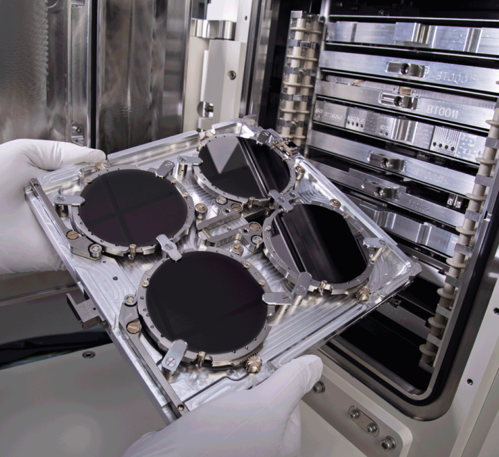
A holder with four 3-inch wafers is one of the possibilities to use in the 10-holder airlock. Image Credit: Raith
Listed below are the features of EBPG Plus
- Safe multi-user environment and various access levels
- Automated wafer and multi-sample exposures
- Availability of automated exposure parameter switching and calibration that enable stable and persistent switching between high throughput and high resolution
- Comes with an easy-to-learn graphical user interface and terminal interface for scripting
- Automated 2- or 10-holder airlock available
- Fast and error-free sample alignment can be performed
- Extremely rapid stage available with very low settling times
- Sophisticated fracturing modes for lowest line-edge roughness
- Highly efficient data processing can be performed with the help of the Firebird technology for the highest pattern fidelity in the shortest time
Users can make the EBPG Plus an extremely adaptable electron beam lithography system that is the ideal choice for use in academia and industries.
Shaping the Future of Nanofabrication
A special combination of modularity, automation and performance is provided by EBPG Plus. Thanks to an intuitive user interface plus automated workflow with optional data pre-processing software, users can concentrate on achieving better outcomes rather than system handling.
EPBG Plus consists of various holders and thus provides uncompromised automation without any limitations for sample or wafer geometry. Moreover, the high-resolution lithography system can be field-upgraded at all times in step with varying demands.
Evolutionary Technology
Raith is the market leader for professional electron beam lithography systems and, therefore, supplies systems that are constantly optimized and enhanced at the leading edge of nanotechnology. Thus, the company gains the experience required to confidently fulfill the demanding needs of industrial clients with ensured uptime and stability. The EBPG Plus enables 24/7 batch mode operation with the least operator input for consistently achieving high output and yield.
Features
- Comes with a direct write performance with an overlay accuracy of ≤5 nm
- Features stable large-area writing with stitching precision of ≤8 nm
- Beam current ranges up to 350 nA
Choose the Right System for Specific Nanolithography Requirements
The EBPG Plus lithography system delivers a high resolution and high throughput. To address the changing requirements of each customer, the system is available in two versions, where both are adaptable.
The EBPG5200 Plus is equipped with full 200-mm writing capability with ultimate stability. The EBPG5150 Plus employs the same universal plinth platform using a 150 mm stage suitable for all R&D and compound semiconductor manufacturing applications.
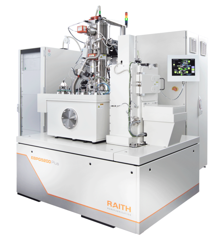
EBPG5200 Plus. Image Credit: Raith
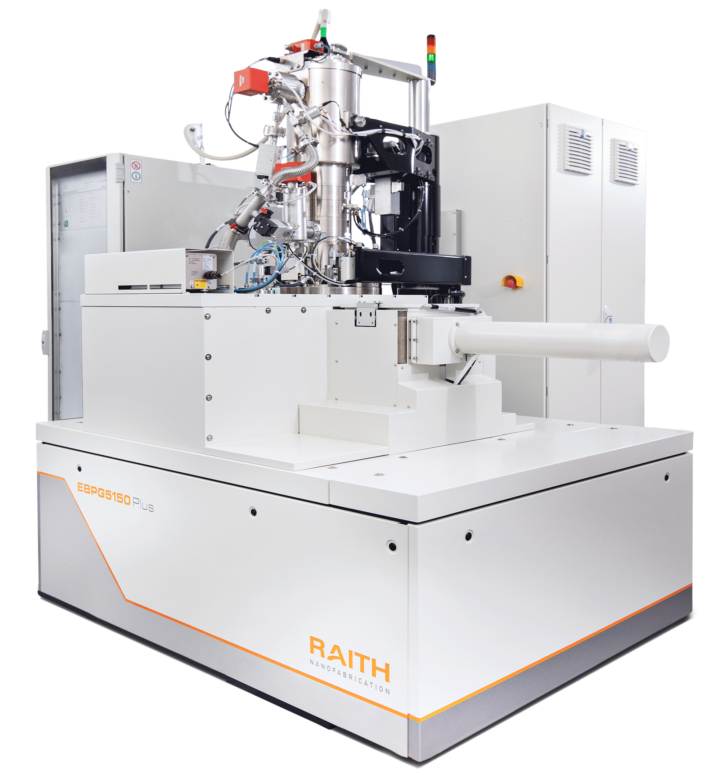
EBPG5150 Plus. Image Credit: Raith
Applications
Photonic CNOT quantum gate. Image Credit: Menno Poot, Yale University, USA
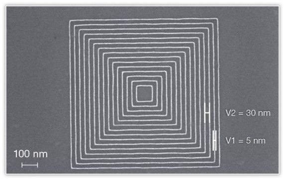
Overlay accuracy of much better than 5 nm demonstrated on a zone plate. Image Credit: CRXO/LBL, Berkley, USA
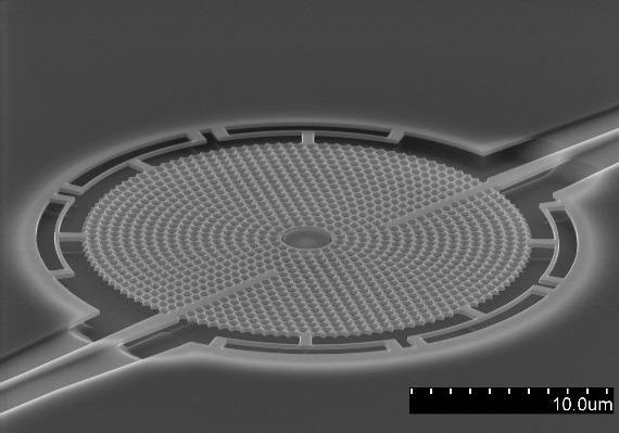
Microdisk resonator embedded into a sunflower-type circular photonic crystal. Image Credit: Xufeng Zhang, Yale University, USA
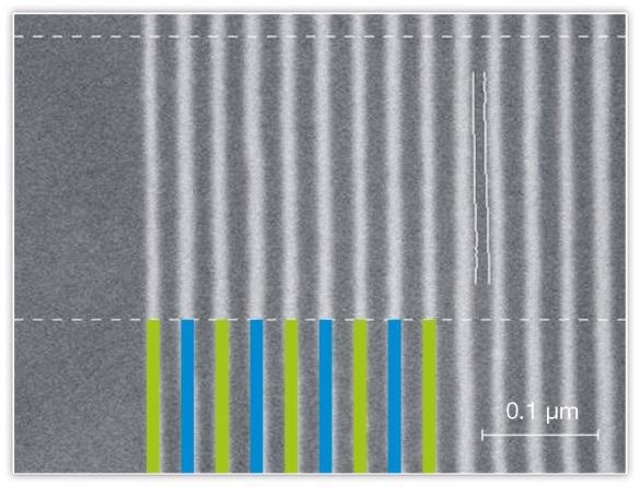
Test pattern with ultra-high resolution lines (5 nm) with 30 nm pitch. Pattern homogeneity is maintained over an entire wafer. Image Credit: Raith
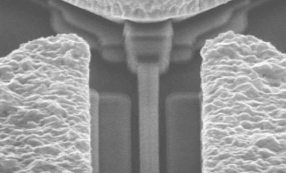
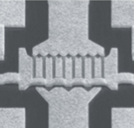
GaAs T gate device. Image Credit: Raith
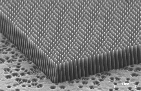
Array of diamond/silicon dioxide nanorods. Image Credit: Sergey Gorelick, Monash University, Australia
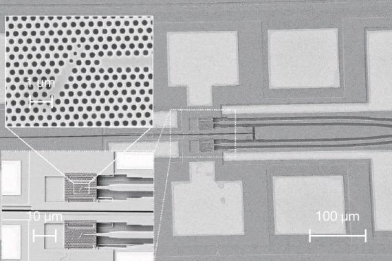
A pair of single-photon nodes in an integrated circuit. Image Credit: M. Petruzzella, Eindhoven University of Technology, Netherlands
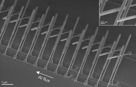
Shadow-grown superconducting islands on InSb nanowires. Image Credit: Sasa Gazibegovic, Delft University of Technology, Netherlands
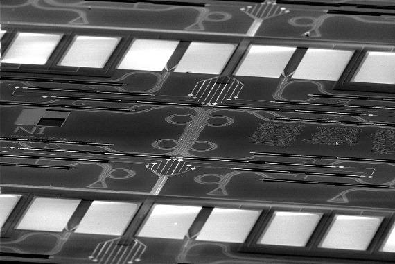
Compound semiconductor application. Image Credit: Raith