May 10 2021
Today, nanofabrication of electronic systems has reached a 1 nm scale (10−9 m). The quick development of nanotechnology and nanoscience currently needs atomic-scale optical spectroscopy to define atomistic structures that will influence the functions and properties of the electronic devices.
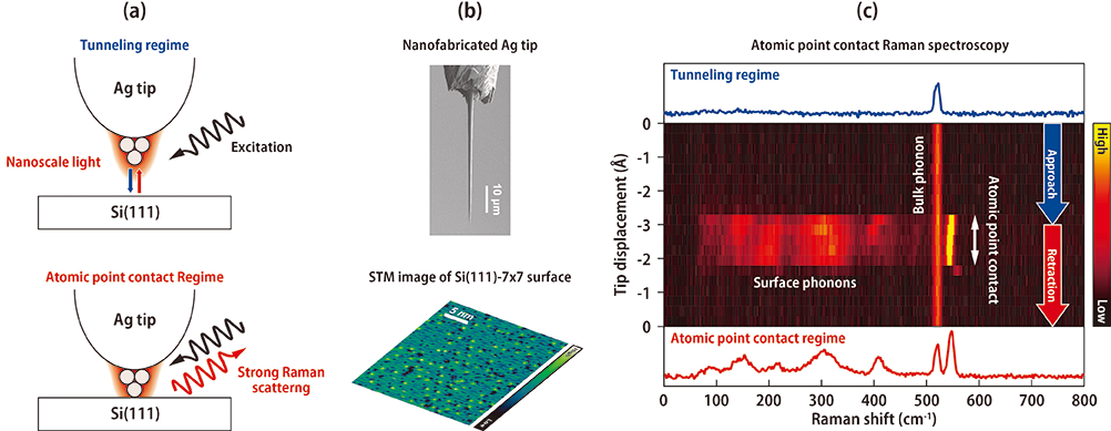 (a) Illustration of the experiment. (b) Scanning electron micrograph of an Ag tip (top) and scanning tunneling microscopy image of the Si(111)-7×7 surface. (c) Atomic point contact Raman spectra. Image Credit: National Institutes of Natural Sciences.
The international research team, led by Takashi Kumagai from the Institute for Molecular Science, observed a massive improvement of Raman scattering facilitated by the development of an atomic point contact between a Si(111)-7×7 reconstructed surface and a plasmonic silver tip. This was realized using advanced low-temperature tip-enhanced Raman spectroscopy that helps perform atomic-scale vibrational spectroscopy.
The newly identified improvement mechanism of Raman scattering will pave the way for atomic-scale ultra-sensitive vibrational spectroscopy to study the surface structures of semiconductors. The developed atomic-scale optical microscopy will also provide opportunities for investigating light-matter interactions at the atomic scale, thus resulting in a new field of discipline in light science and technology.
The super integration of electronic devices has reached a 1 nm scale, calling for analytical techniques that can analyze structures and defects at the atomic scale more thoroughly. The progression of scanning near-field optical microscopy has enabled nanoscale imaging and nanoscale chemical studies.
In the recent past, it was demonstrated that the spatial resolution of this method reached the atomic scale. Tip-enhanced Raman spectroscopy, in particular, had attracted a great deal of interest as ultra-sensitive chemical microscopy. But to acquire a Raman signal from the surfaces of semiconductors, the sensitivity had to be further improved.
The researchers used advanced low-temperature tip-enhanced Raman spectroscopy, designed in association with Fritz-Haber Institute, to achieve the vibration spectra from the surface of silicon.
Tip-enhanced Raman spectroscopy uses a powerful light-matter interaction between a material and nanoscale light—that is, localized surface plasmon resonance—produced at an atomically sharp metallic tip.
The team noted that a reconstructed Si(111)-7×7 surface and the formation of atomic point contact of a silver tip result in a massive improvement of Raman scattering. The experiment is shown in the above image.
A sharp silver tip produced by the focused ion beam (as shown in Figure 1b, top) is shifted toward the surface of the silicon (as illustrated in Figure 1b, bottom0, while tracking the Raman spectra from the junction. Figure 1c also shows the waterfall plot of the acquired Raman spectra in which the color scale the Raman intensity and the horizontal axis the Raman shift.
When the tip remains in the tunneling regime, the optical phonon mode of the bulk silicon alone is visualized at 520 cm−1. But when there is an atomic point contact between the surface and the tip, the powerful Raman scattering from the surface phonon modes appears abruptly. These modes vanish again when the tip is shifted away from the surface and the atomic point contact is ultimately broken.
The researchers also showed that such an atomic point contact Raman spectroscopy (APCRS) is capable of resolving the atomic-scale structures of the surface of the silicon. However, the Raman spectrum is not the same when it is captured at an atomic step of the surface. Moreover, the typical vibration modes can be visualized selectively at the locally oxidized location, denoting the atomic-scale chemical sensitivity of atomic-point-contact Raman spectroscopy.
Earlier, it was assumed that a plasmonic nanogap is required to achieve the ultra-high sensitivity in tip-enhanced Raman spectroscopy, which generally needs a metal substrate. And this imposed a severe restriction on quantifiable specimens.
The findings of the major Raman enhancement upon the formation of atomic point contact will extend the possibility of atomic-scale vibration spectroscopy, which is relevant to non-plasmonic specimens, and the excellent chemical sensitivity will be achieved for several other materials. The results also indicate that atomic-scale structures play a crucial role in metal–semiconductor hybrid nanosystems to influence their optoelectronic characteristics.
Journal Reference:
Liu, S., et al. (2021) Atomic Point Contact Raman Spectroscopy of a Si(111)-7 × 7 Surface.
Nano Letters. doi.org/10.1021/acs.nanolett.1c00998.
Source: https://www.ims.ac.jp/en/