In this interview, AZoNano talks to Eduard Weichselbaumer, Senior Executive at PrimeNano, about the work they do in the Atomic Force Microscopy Field and the advances the company is making.
Please could you give an overview of PrimeNano and the work you undertake within the Atomic Force Microscopy field?
PrimeNano was founded by two Stanford University professors: ZX Shen and Mike Kelly with exclusively licensed atomic force microscopy microwave technology. We are the most exciting new addition to the AFM world that has otherwise reached maturity.
Our latest product, the ScanWave™ Pro, has demonstrated unprecedented sensitivity to the electrical properties of material such as dielectrics and semiconductors. Our solutions work in conjunction with established AFM systems and techniques, so we are an easy extension for the AFM community.
PrimeNano is a modern Silicon Valley success story of taking a university invention and creating a valuable solution around it. We are growing in leaps and bounds having doubled every couple of years since the formation of the company 7 years ago.
2020 and 2021 will be banner years as we are bringing to market several products some in areas never before served such as cryogenic microwave microscopy.
What is the importance of microwave microscopy?
Microwave microscopy opened a new frontier in AFM capability, that of imaging the electrical properties of material. These electrical property images can be acquired at the same time as surface topography images and be combined for a comprehensive understanding of many types of materials.
Microwaves are non-invasive and can penetrate material adding another dimension to AFM, that of imaging of buried structures. Microwaves also work in contact or non-contact mode and even though the electrical properties are probed, grounding or other electrical contact to the sample is not needed.
PrimeNano has revolutionized Scanning Microwave Impedance Microscopy to enable the characterization and process control of the electrical properties of materials at the nanoscale.
ScanWave™ is used in industry and research to expand the capabilities of traditional AFM into the nanoscale material properties realm. The sensitivity of the Pro is at the limits of what can be measured, and it is streamlined for ease of use.
The ScanWave™ technology works without any electrical contact to the sample (i.e., grounding), can image through hundreds of nanometers of material and requires little to no sample prep.
Please could you discuss the main principles/procedures of ScanWave™ (Scanning Microwave Impedance Microscopy)?
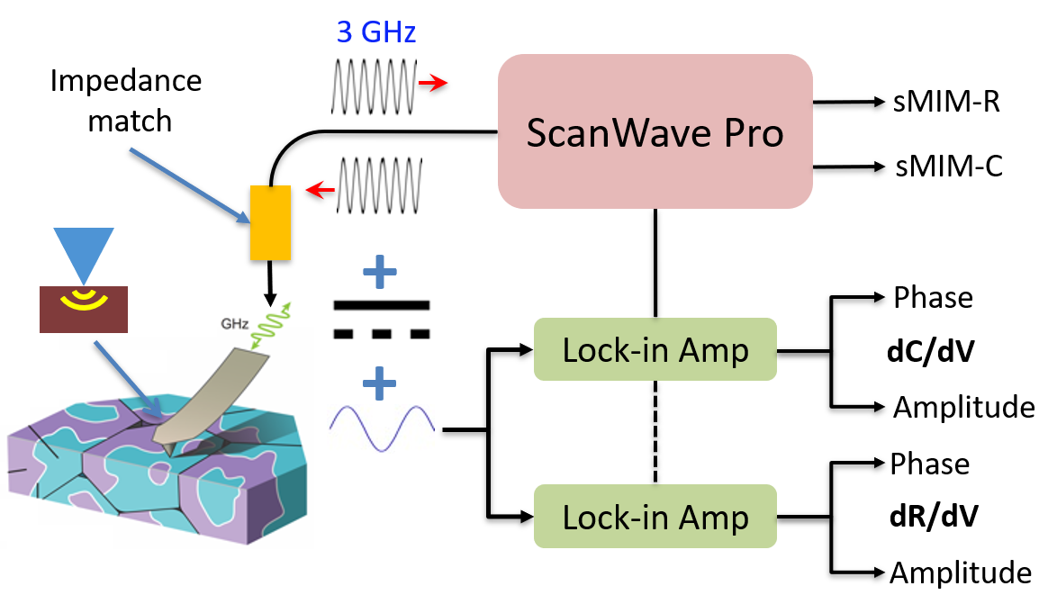
ScanWave™ uses microwaves to non-invasively probe material to determine electrical properties such as dielectric constant and conductivity.
A special cantilever manufactured by PrimeNano using a proprietary patented MEMS process is used in an AFM system to deliver microwaves to the probe tip mounted on any of a number of common AFM platforms.
The ScanWave system generates and delivers the microwaves to the tip using a shielded waveguide and the reflected signal is collected and used to measure localized variations in the electrical properties of material with nanoscale resolution.
Following on from the previous question, what are the possibilities that this technique provides?
PrimeNano has developed room temperature and ultra-low temperature solutions that open up the possibilities in many emerging technologies such as quantum computing, semiconductors, ferroelectrics and more.
We offer 3 low temperature solutions that specifically address the needs of materials research at the nanoscale be it in ultra-high vacuum and high magnetic field cryogenic measurements, ultra-low temperature (<100 mK), stand alone or integrated in a cluster.
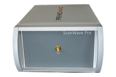
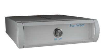
The ScanWave Pro's Electronics Box (top) and Power Supply (bottom)
What applications does the technology serve and enable?
Because of the simple nature of the setup needed for ScanWave™ and the vast variety of materials that can be imaged, the applications space spans many areas of nanotechnology.
Semiconductors, carbon nanotubes, dielectrics, ferromagnetic materials, quantum materials can all be imaged for their electrical properties with nanoscale precision.
Examples of use cases include CNT characterization (ScanWave can determine conductivity of individual CNT’s), semiconductor dopant concentration and type (n or p), ferromagnetic material phase and conductivity variations at the nanoscale, Nano Moiré patterned material and many more.
How is the ScanWave Pro well-suited to this type of analysis/What are the key features of the ScanWave Pro that make it well-suited to performing this type of analysis and what sets it apart from competitors?
Over the last few years, PrimeNano invested significantly in R&D to produce the Pro model which has the highest sensitivity of any such system in the field by an order of magnitude or more. We can measure the lowest capacitance samples commercially available with < 0.1 aF capacitance sensitivity.
The lateral resolution of the Pro is also in the deep nanoscale at sub 10 nm, an industry first and only such capability for electrical properties of the material. The probes themselves are of a custom design and manufactured using an IP protected MEMS process.
We have ensured that the signal integrity is maintained from the source to the very tip of the probe. Combined with low noise electronics we offer the best S/N in the industry, also improved dramatically in the Pro.
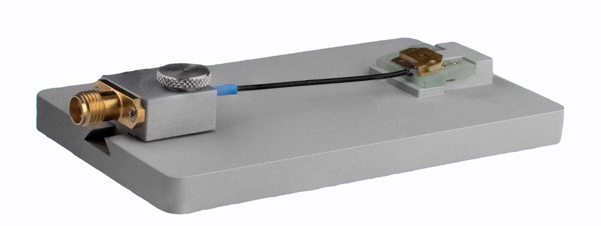
PrimeNano's Probe Loading Station
What does the future hold for PrimeNano and the microwave microscopy field?
As with many young technologies, there is tremendous growth and excitement around ScanWave™ right now. We are offering to the mature AFM user community a boost in capability and a path for growth that complements all the existing knowledge and infrastructure of the AFM ecosystem.
We expect to broaden our applications space as our latest products address new and previously unresolved challenges. In addition, we are implementing automation and quantification of the ScanWave information which we expect to take us into high volume manufacturing uses such as materials metrology and process control.
Where can readers find more information?
There is a wealth of information about the company at the PrimeNano Website: primenanoinc.com
About the interviewee
Eduard Weichselbaumer is a senior executive with more than 20 years of experience building and managing companies all around the globe, from small startups to Nasdaq listed companies. He combines a background in BA and EE having led the operational, engineering, as well as sales and marketing efforts of many organizations.
Before joining PrimeNano, he held leadership roles in LSI Logic, Synopsys Semiconductor IP business, Artisan Components (Nasdaq: ARTI), Virage Logic (Nasdaq: VIRL), SOISIC and CEITEC SA. He was also the founding CEO of a startup semiconductor company with a 6” wafer fabrication plant and more than 100 chip designers.

This information has been sourced, reviewed and adapted from materials provided by PrimeNano.
For more information on this source, please visit PrimeNano.
Disclaimer: The views expressed here are those of the interviewee and do not necessarily represent the views of AZoM.com Limited (T/A) AZoNetwork, the owner and operator of this website. This disclaimer forms part of the Terms and Conditions of use of this website.