Feb 24 2010
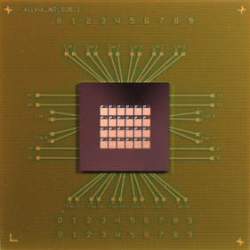
ALLVIA, the first through-silicon via (TSV) foundry, has integrated embedded capacitors on Silicon Interposers, a key interface between a silicon device and an organic substrate needed for managing high interconnect densities.
Capacitance values higher than 1,500 nF/cm2 have been achieved for the embedded capacitors developed for delivering power to the devices. 3D integration with ALLVIA's through-silicon via technology allows much closer access to high value capacitors than previously possible, leading to a much higher level of electrical performance.
 ALLVIA Interposers
Thin film capacitors
Thin film capacitors without TSVs have been used previously. However, with the interconnect inductance being high, benefits of thin film capacitors have not been fully realized. TSV interposers with embedded capacitors provide the shortest electrical path between devices and power supply decoupling capacitors. TSVs with their very low inductance interconnects thus will enable very high electrical performance when integrated with embedded thin film capacitors.
ALLVIA's silicon TSV interposers enable interconnect pitch matching between a high-density IC chip and an organic or a ceramic substrate. Further, they provide a very low stress interconnect to Si ICs that use low-k dielectrics. These benefits make ALLVIA's interposers an attractive solution for advanced packaging of next generation logic devices.
"The capacitance value of 15 nanofarads per millimeter square is not a limit of our process and we think that the integration of capacitors with TSVs and silicon interposers is a technological breakthrough. The capacitance from the die or package can now be transferred to the interposer," commented Sergey Savastiouk, CEO of ALLVIA.
Silicon Interposers
In January, ALLVIA announced that it had completed the integration of a silicon interposer between a semiconductor die and an organic or ceramic substrate and had completed reliability testing. This 3D integration of substrates is made possible with ALLVIA's through-silicon vias. Samples and reliability data are being made available to interested customers.
Source: http://www.allvia.com/