AZoNano speaks with Ping Wang, Ph.D., about his involvement in the graphene hBN advancement that could boost the development of next-generation electronic and quantum devices. Here, we discuss the synthesis methodology behind this latest advancement.
Please could you introduce yourself and tell us about your current position and research activities?
My name is Ping Wang, and I am a postdoctoral research fellow in the Department of Electrical Engineering and Computer Science, University of Michigan. My research interest focuses on wide bandgap III-nitride semiconductor materials and devices, including GaN-based III-nitrides, and the emerging ferroelectric ScAlN and two-dimensional hBN.
Could you summarize the results of your recent research?
We demonstrated the unidirectional growth of monolayer hBN on graphene substrates, for the first time, which exhibit large-scale and single-periodicity moiré superlattice, and excitonic emission in the deep-ultraviolet spectrum range.
This achievement is a pivotal step for the controlled synthesis of ultraclean, wafer-scale, atomically ordered 2D quantum materials, as well as the fabrication of 2D quantum electronic and optoelectronic devices.
What characteristics of hexagonal boron nitride (hBN) make it particularly useful for 2D material applications?
hBN is isostructural to graphene, referred to as “white graphene”. Monolayer hBN has been theoretically predicted to have an ultrawide direct bandgap of ~8 eV, while multilayer hBN has an indirect bandgap of ~5.9 eV. Therefore, hBN is the thinnest insulator in the world and has been considered a fundamental building block of 2D electronic and optoelectronic devices.
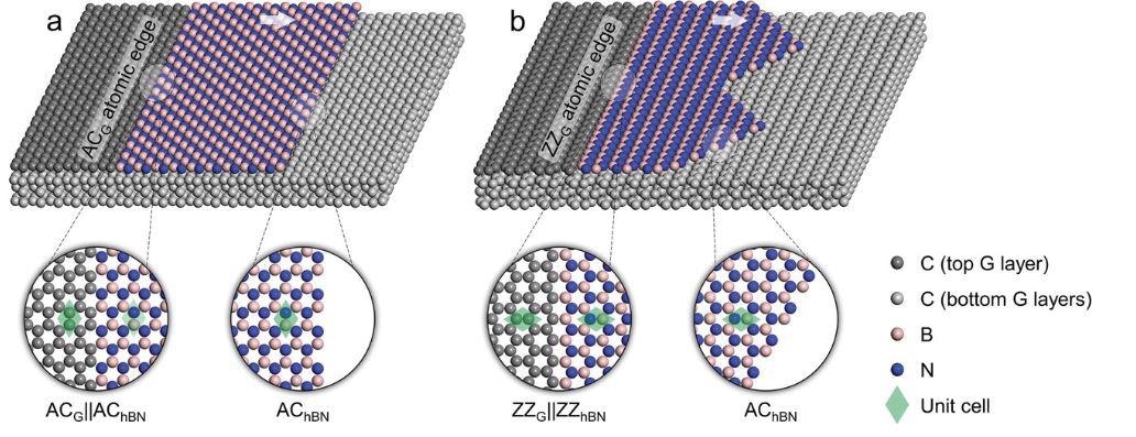
Concept and demonstration of interface-mediated synthesis of monolayer hBN. a,b) Schematics of monolayer hBN grown along the armchair (ACG) (a) and zigzag (ZZG) (b) graphene atomic edges, forming straight and jagged nanoribbons, respectively. All growth fronts of monolayer hBN are terminated with AChBN edges. The magnifications show the atomic configurations of the ACG||AChBN and ZZG||ZZhBN in-plane interfaces, and the AChBN growth fronts. The white arrows point to the growth direction. © Wang, P., et al (2022)
What is the significance of optimizing the fabrication of single-layered hBN? What sectors would benefit the most from this?
To obtain a useful product, you need consistent, ordered rows of hBN atoms that align with the graphene underneath, and previous efforts weren’t able to achieve that. Some hBN went down neatly, but others were disordered and randomly aligned.
Optimizing the growth or synthesis process will give us large-scale atomically ordered single-layer hBN, which are essential for future scalable integration and mass production.
This kind of single-layer hBN can be used in high-efficiency ultraviolet optoelectronics, high-power and low-power-loss electronics, quantum information, the exciting 2D van der Waals devices, as well as energy conversion and storage devices.
The bonding between hBN and graphene is said to facilitate a ‘treasure trove’ of properties. What are some of the stand-out characteristics?
Vertically stacked hBN/graphene (hBN/G) van der Waals (vdW) heterostructures have been successfully employed to produce emergent properties, such as quantum Hall effect, Hofstadter butterfly spectrum, and plasmon and phonon polaritons.
Complementary to the vertical hBN/G vdW heterostructures, the in-plane version forms covalent hBN/G heterostructures with equally attractive properties, such as transitions between semiconducting, half-metallic, and metallic phases, spin polarization magnetism, and exotic electronic states, or even the possibility to reconstruct electronic interfaces similar to those observed in oxide heterostructures.
The scope of these fascinating properties could be radically expanded by demonstrating epitaxially grown monolayer hBN on graphene with superior structural, electrical, and optical properties, as well as precise control of both the hBN/G out-of-plane and in-plane monolayer interfaces.
Building larger graphene-hBN sheets with molecular beam epitaxy
Building larger graphene-hBN sheets with molecular beam epitaxy. © University of Michigan Engineering
What were the major challenges you had to overcome in this investigation? Were any particular methodologies or equipment particularly influential in obtaining successful results?
At the beginning of this investigation, we obtained similar results to previous reports, i.e., monolayer and multilayer hBN are randomly distributed on the graphene substrates without selectivity.
To realize the synthesis of uniform and unidirectional monolayer hBN, we need to control the growth process from the initial nucleation, i.e., graphene-hBN in-plane nucleation interface formation. However, there is a myriad of possible graphene-hBN in-plane interfaces. If the growth only happened from one of these interfaces, unidirectional monolayer hBN growth can be achieved.
From previous theoretical calculations, we found that these interfaces have different energetic stability. From this point, we developed an interface-mediated growth concept. We performed hBN growth at an ultrahigh growth temperature of 1600 degrees Celsius using an ultrahigh temperature Veeco GENxplor molecular beam epitaxy system.
With such high growth temperature, all other graphene-hBN interface formation is dramatically suppressed; therefore, large-scale unidirectional monolayer hBN was achieved on the graphene substrates.
What are the next steps for this area of research?
Despite the unique characteristics of hBN for promising applications in electronic and optoelectronic devices, more research must be accomplished to improve the reliability and take it from laboratory to industrialization.
In-depth understanding of the fundamental growth dynamics and thermodynamics, as well as the effect of the substrates, is essential for the development of hBN and related devices. Furthermore, to satisfy the wide range of hBN applications, the layer thickness must be controlled precisely from monolayer to multilayer on a large scale with high uniformity and crystal quality.
Additionally, epitaxially grown vertical and in-plane hBN-based heterostructures with crisp, clean, and atomically ordered interface would be of great importance for improving device performance. However, this remains a difficult and challenging task.
In the future, we will try to combine theoretical approaches and experimental approaches to further develop simple and scalable methods for controllable synthesis of hBN-based heterostructures, which is not restricted to the hBN 2D heterostructures, but also the combination with conventional III-nitrides.
With these achievements, hBN-based filed effect transistors, ultraviolet light-emitting diodes, and more will be further studied.
© ktsdesign/Shutterstock.com
How do you predict the research landscape of quantum materials and technologies to change over the next 30 years? What impact on the industry might this have?
Next-generation electronic and optoelectronic devices will benefit from foldability/bendability/rollability, high durability, and high space efficiency. These devices need large-scale flexible and extendable materials with excellent metallic/semiconducting/insulating properties, such as graphene, hBN, and other 2D materials.
It is well known that the dimension of transistors is reaching the scaling limit, and unprecedented obstacles are at the corner, but we are not prepared for the end of Moore’s law. On the other hand, the power consumption of the transistor needs to be further reduced, especially in small devices. Therefore, new advanced quantum materials should be developed to address the challenges in the next-generation semiconductor devices. I believe the emerging quantum materials will bring a revolutionary change to the world in the next 30 years.
Currently, most commercial devices are still based on mature Si technology. To realize mass production for the next-generation electronic and optoelectronic devices and systems, the chip manufacturers need to develop new processes and technology to meet the manipulation of quantum materials.
In your opinion, what was the most exciting aspect of this investigation?
The most exciting aspect of this research is that scalable and unidirectional growth of monolayer hBN on graphene has been achieved by modulating the formation of the interface at atomic scale through a simple method——ultrahigh temperature growth. And a giant direct bandgap renormalization for monolayer hBN has been experimentally and theoretically revealed.
About Ping Wang Ph.D.
 Ping Wang is a research fellow in the Electrical Engineering and Computer Science department at the University of Michigan from 2018. His research interests are on the growth of emerging wide bandgap III-nitride semiconductors and their electronic and optoelectronic device applications. In this work, Prof. Zetian Mi and he constructed the concept together, and performed the synthesis of monolayer hBN.
Most recently, they also demonstrated, for the first time, fully epitaxial ferroelectric ScAlN/GaN heterostructures, which is another rising star for III-nitrides family. They will continuously work in the III-nitride semiconductors and devices and try to make more progress to change the world.
Disclaimer: The views expressed here are those of the interviewee and do not necessarily represent the views of AZoM.com Limited (T/A) AZoNetwork, the owner and operator of this website. This disclaimer forms part of the Terms and Conditions of use of this website.