A novel nanoanalytical technique developed by scientists from Thermo Fisher Scientific and the University of Technology in Sydney, Australia, enables researchers to analyze the composition of a wide range of materials and visualize the elemental distribution in 3D. With this new development, further insights into the structure-function relationship of advanced nanostructured materials can be obtained.
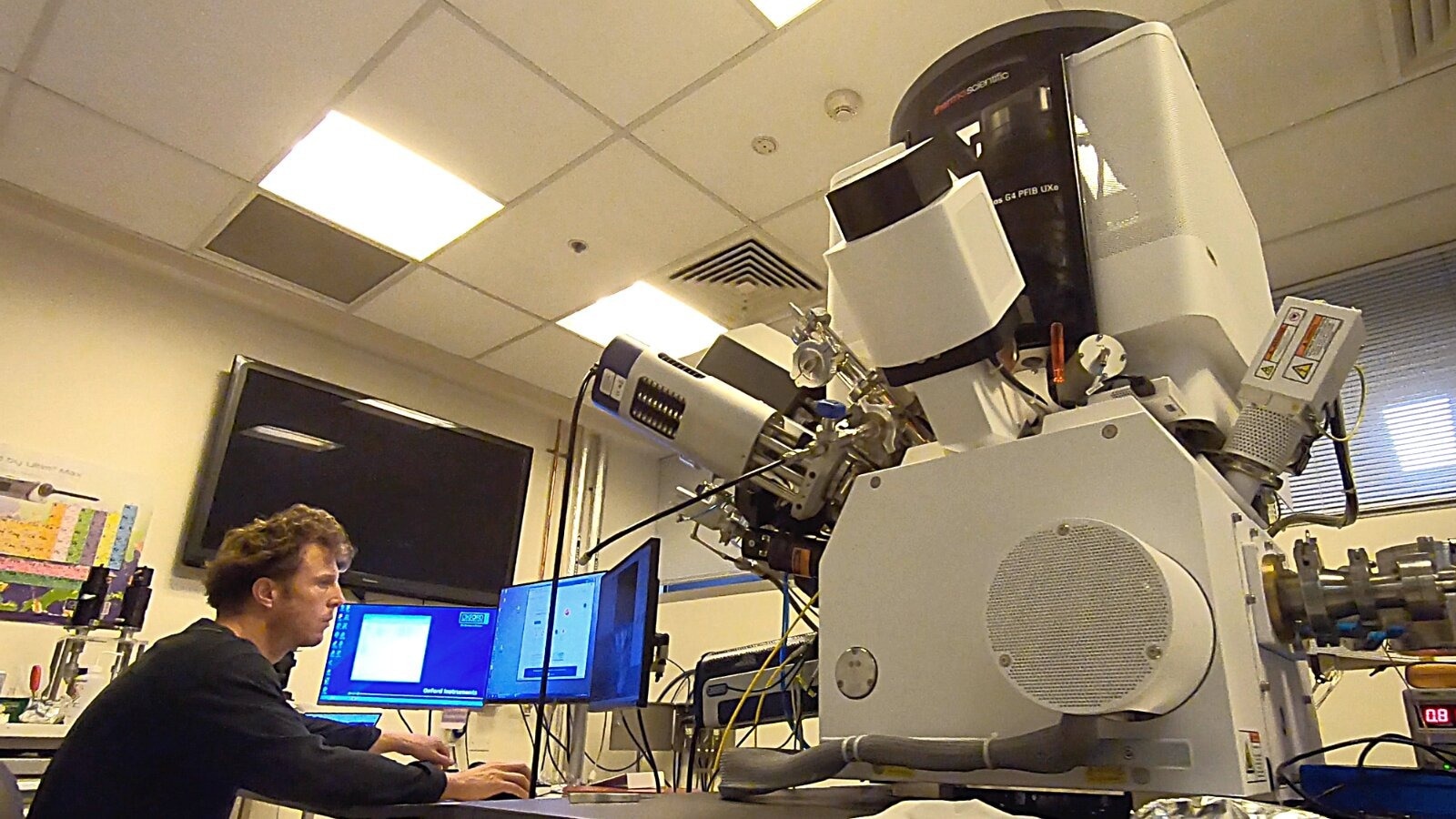
Dr. John Scott, University of Technology Sydney with the plasma FIB dual beam microscope. Image Credit: Milos Toth
Detailed mapping of the distribution of chemical elements in 3D underpins many advanced manufacturing processes used in microelectronics, additive manufacturing, chemical engineering, energy storage, and many others.
Modern materials research is increasingly reliant on nanoscale elemental analysis. Rapid and highly sensitive examination of the elemental composition has become a requirement when studying the real 3D structure and composition of nanomaterials, such as catalysts, semiconductor nanodevices, and nanoparticles with advanced optical properties. In many advanced applications, even slight changes in the elemental composition and distribution can drastically alter the relevant properties of the material.
Visualizing Nanoscale Composition in 3D
Currently, some of the best-suited techniques for nanoscale elemental analysis combine scanning transmission electron microscopy (STEM), spectroscopy, and tomography. Such a combination offers nanometer-scale spatial resolution, high elemental sensitivity, and the ability to reveal the full 3D structure of the studied object.
Electron tomography produces a 3D reconstruction of the material's structure by incrementally adjusting the imaging angle of the sample, thus creating a tilt series of digitally processed images to render a 3D image of the imaged sample volume.
Energy-dispersive X-ray spectroscopy (EDX) performed simultaneously with STEM at different tilt angles is an effective method for 3D physicochemical analysis of nanomaterials due to its capability of atomic-scale imaging and comprehensive elemental analysis of the sample. Similarly, STEM electron energy-loss spectroscopy (STEM-EELS) tomography enables scientists to study the functional properties of nanomaterials in 3D by revealing the chemical state of the elements present in the material.
Unfortunately, these methods usually require long acquisition times, which hinders their use in high-throughput applications, such as nanomaterial analysis in industrial settings or when investigating dynamic processes in materials.
High-Throughput 3D Elemental Analysis in Nanomaterials
Comprehensive high-throughput 3D characterization of nanomaterials, including chemical elemental analysis and imaging data, requires advanced instrumentation with dynamic high-resolution imaging capabilities and fast quantitative elemental analysis data acquisition.
Recently, researchers from Thermo Fisher Scientific in the USA and the University of Technology in Sydney, Australia, developed a novel analytical method based on focused ion beam (FIB) tomography that can meet these requirements. FIB systems use a tightly focused ion beam (typically gallium ions) that, when operated at high beam current, can be used to locally sputter or mill a sample surface by removing the topmost atomic layer of the material.
Initially, FIB milling found use as a lithographic technique for nanomaterials processing in various microelectronics and micromechanics applications. Following recent technological advances, the method is now widely used as a tomographic technique in materials science and biomedical research. Due to the ion bombardment of the sample surface with high-energy ions (energy range above a few tens of electron volts), some of the sputtered surface atoms leave the sample surface in an electronically excited state and emit light at characteristic wavelengths.
The international research team harnessed this bombardment-induced light emission to combine the high spatial resolution and high sensitivity of the 3D FIB tomography with the versatility of fluorescence spectroscopy.
Diffraction-Unlimited Fluorescence Spectroscopy
The FIB-induced fluorescence spectroscopy (FIB-FS) nanoanalytical method offers many improvements over other 3D characterization methods, including spatial resolution of approximately 15 nanometres (exceeding the micron-scale resolution of the EDX technique and comparable to the resolution of STEM-EDX). Notably, the FIB-FS technique can reliably detect light elements, such as hydrogen, helium, and lithium, which is a challenge for X-ray spectroscopy-based methods.
Integrating elemental analysis with the ion milling process optimizes the characterization process and allows a single surface scan to be completed in approximately one second. The rapid data acquisition permits the collection of several thousand tomographic cross-sections and the creation of a high-resolution 3D image stack representing the elemental composition of the studied material.
High Spatial Resolution Combined with Trace-Level Sensitivity
To demonstrate the full capabilities of the FIB-FS technique, the researchers characterized a sample with a well-defined nanostructured material comprising three GaAs quantum wells with thicknesses of 3.5, 5, and 8 nanometers embedded in epitaxial AlGaAs layers. Additionally, the versatility of the techniques was demonstrated by performing a 3D elemental analysis of a lithium-nickel-manganese-cobalt-oxide cathode used in Li-ion battery manufacturing.
In this case, the FIB-FS method detected potassium and lithium at concentrations of 3.9 and 0.8 ppm (part per million), thus proving its ability to detect trace-level impurities and additives in functional materials.
In the future, the scientists expect to improve the analytical performance of the FIB-FS technique by optimizing the ion beam parameters and increasing the photon detection efficiency, making the technique appealing for a wider range of applications.
Continue reading: How Elemental Analysis Supports Nanomaterials Research
References and Further Reading
Budnik, G., et al. (2022) Nanoscale 3D Tomography by In-Flight Fluorescence Spectroscopy of Atoms Sputtered by a Focused Ion Beam. Nano Letters, 22(20), pp. 8287-8293. doi.org/10.1021/acs.nanolett.2c03101
Thorn, S. (2022) New characterization methods developed to identify light elements. [Online] www.tmos.org.au. Available at: https://www.tmos.org.au/
Han, Y., et al. (2021) Deep learning STEM-EDX tomography of nanocrystals. Nat Mach Intell, 3, pp. 267–274. doi.org/10.1038/s42256-020-00289-5
Hassan, D., et al. (2019) Focused Ion Beam Tomography. In I. Ahmad, & T. Zhao (Eds.), Ion Beam Techniques and Applications. IntechOpen. doi.org/10.5772/intechopen.88937
Disclaimer: The views expressed here are those of the author expressed in their private capacity and do not necessarily represent the views of AZoM.com Limited T/A AZoNetwork the owner and operator of this website. This disclaimer forms part of the Terms and conditions of use of this website.