The global transmission electron microscope market is rapidly expanding due to the increasing demand for analytical and structural characterization of nanostructured materials and is projected to reach $1.0641 billion by 2028.
Transmission electron microscopes (TEMs) use an electron beam to create magnified images of specimens, allowing for the visualization of compositional, morphologic, and crystallographic details at the atomic level.
Compared to optical microscopes, TEMs can magnify nanostructures up to 50 million times as the wavelength of electrons is about 100,000 times shorter than light.
Using Transmission Electron Microscopes in Nanotechnology
The transmission electron microscope has undergone significant advancements and has become a highly advanced device with extensive use in various scientific fields.
Its exceptional capability to offer detailed information about the chemical and structure composition of materials, even at atomic levels, has made it an essential instrument for studying and manipulating nanostructured materials.
TEMs help better understand 3D atomic arrangements and their impact on material properties, which can improve the quality of nanoparticles and accelerate the application of technologies like heat-assisted magnetic recording (HAMR).
TEM is used to visualize intracellular components of samples up to 1 nanometer, providing insights into the morphological structure of small organisms, such as viruses and bacteria, and cellular inclusions through 3D imaging.
TEM is a widely adopted tool in the semiconductor industry and is crucial for developing new nanostructured semiconductor materials and ensuring the quality of existing and new nanoscale electronic devices.
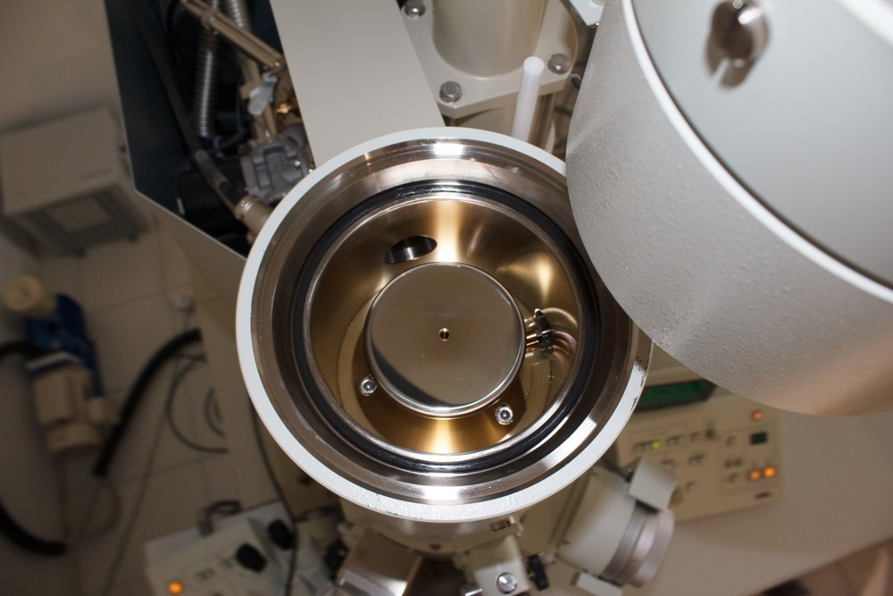
Image Credit: Pvince73/Shutterstock.com
Recent Developments Transmission Electron Microscope Market
Innovation Center for Microscopy Solutions
Hitachi High-Tech Corporation has established an "Advanced-Technology Innovation Center Naka" in Hitachinaka, which will serve as a center for electron microscopy and probe microscopy demonstrations and collaborations with customers.
The center aims to promote the development of new solutions for analytical system products and boost integrated solution development in the electron microscopy and probe microscope-related sectors through closer customer cooperation.
Nanostructured Electronic Devices and Materials Characterization
In a study published in Small, researchers demonstrated a new application of TEM for fabricating in-plane heterojunctions of few-layer MoS2. MoS2 is a promising material for energy harvesting, nanoelectronics, and valleytronics.
The researchers used in situ folding, scrolling, etching, and restructuring techniques to create nanoscale heterojunctions in the TEM. This successful creation of lateral heterointerfaces suggests that it may be possible to design and fabricate relevant geometries for use in quantum, energy storage, and optoelectronic devices using TEM.
Affordable and User-Friendly Cryogenic Transmission Electron Microscope
Developing a user-friendly and low-cost cryogenic transmission electron microscope (cryo-TEM) is an ongoing research priority in microscopy.
Cryo-TEM is an expensive technology, but making it affordable would significantly boost visualizing and sizing nanoparticles, imaging weakly bonded materials and analyzing proteins that would otherwise degrade under standard electron microscopy conditions.
Current Global Market of Transmission Electron Microscope
According to a report, the global market for transmission electron microscopes was valued at $825.44 million in 2022 and is projected to reach $1,064.09 million by 2028, expanding at a CAGR of 4.32 % over the forecast period.
Market Drivers
The growing emphasis on nanotechnology is driving the transmission electron microscope market. Governments and multiple industries are investing heavily in nanotechnology for its potential applications in food, medicine, biomaterials, electronics, and microfabrication. These applications will boost TEM market growth.
For example, nanotechnology is increasingly being integrated into developing stronger and lighter metals for various applications. This has led to increased utilization of TEMs, as they provide better visibility of material structure and composition.
Challenges
The initial investment cost of these microscopes is high, and they heavily rely on corporate funding. In addition, import duties and other taxes imposed by governments increase the cost price of the final product and limit the market growth.
The preparation of thin specimens to allow electrons to pass through is difficult, which has hindered the growth of the transmission electron microscope market.
Regional Highlights
North America is a significant market for the transmission electron microscope, driven by major industry players like JEOL, who produce advanced transmission electron microscopes. The region also benefits from many research facilities and educational institutions, such as The Microscopy Society of America, which supports research and innovation in microscopy.
The growth of research and development facilities in the region has positively impacted the European market for transmission electron microscopes. Initiatives such as the European Microscopy Society have aimed to promote advanced microscopy in Europe, focusing on improving methodology and instrumentation and exploring new applications of various microscopy techniques.
The Asia Pacific region is a significant market for transmission electron microscopes, with notable contributions from China, Japan, and India. The market has experienced growth due to the low cost of raw materials, increased government funding for research and development, and growing demand for ultra-thinned silicon wafers, particularly in the semiconductor industry.

Image Credit: tadamichi/Shutterstock.com
Key Players in the Transmission Electron Microscope Market
Key players such as JEOL, Hitachi High-Technologies Corporation, TESCAN, Leica Microsystems and Thermo Fisher Scientific dominate the global transmission electron microscope market.
These companies have strengthened their market position by implementing strategies such as introducing new TEM models, forming partnerships and collaborations, acquiring or merging with other companies, and establishing joint ventures.
JEOL
JEOL is a leading manufacturer of transmission electron microscopes with over 70 years of experience in the field. They offer high-performance TEMs for life and material sciences, featuring ultrahigh-resolution optics for atom-to-atom imaging and analytical characterization down to the picometer level.
The 200kV NEOARM "Atomic Resolution Imaging & Analytical Electron Microscope" developed by JEOL enables atomic-resolution imaging at accelerating voltages ranging from 30 kV to 200 kV. It is particularly suited for high-resolution imaging of light element-containing materials and electron-beam-sensitive specimens.
Hitachi High-Technologies Corporation
Hitachi offers advanced scientific tools such as TEMs, SEMs, microscopes, and analyzers.
Hitachi's 200 kV aberration-corrected TEM/STEM microscope HF5000 perfectly synchronizes efficient, high-resolution imaging and analytical performance. It offers a spatial resolution of 0.078 nm in STEM mode, high specimen-tilt capacity, and large EDX detectors within a single objective lens configuration, making it a unique and versatile tool for various applications.
TESCAN
TESCAN is a leading provider of advanced scientific instruments. Their 4D STEM instrument, TESCAN TENSOR is a groundbreaking near-UHV microscope that offers integrated, precession-assisted and analytical capabilities.
TENSOR enables real-time multimodal nanoscale characterization of material properties, including morphology, chemistry and structure. Its ease of use, coupled with its advanced features, makes it a powerful tool for applications in material science, semiconductor research and crystallography.
Leica Microsystems
Leica Microsystems, a prominent provider of scientific and medical imaging equipment, offers advanced sample preparation equipment for Cryo-Transmission Electron Microscopy (Cryo-TEM) instruments. Their Leica EM CTD provides fast and reliable cryo-tool drying for efficient Cryo-EM workflows, while the EM GP2 offers an automatic plunge freezer.
Thermo Fisher Scientific
Thermo Fisher Scientific offers a range of TEM products that simplify and automate operations for improved imaging and analysis. Its TEM products are versatile and suitable for multi-user and multi-disciplinary environments with multiple applications in a single system.
The Thermo Scientific Spectra 300 S/TEM is one of the fastest and most reliable TEM, ideal for semiconductor material research and failure analysis.
Future of Global Transmission Electron Microscope Market
The Global Transmission Electron Microscope market is expected to experience significant growth between 2023 and 2029, with a steady rise in 2022.
The market offers ample growth opportunities for vendors by developing new transmission electron microscope forms and increasing semiconductor research and mining applications. However, the market participants may face challenges due to the rising demand for multipurpose electron microscopes.
References and Further Reading
Technavio. (2022). Transmission Electron Microscope Market by Application, End-user, and Geography - Forecast and Analysis 2022-2026. [Online]. Available at: https://www.technavio.com/report/transmission-electron-microscope-market-industry-analysis
MarketWatch. (2023). Global "Transmission Electron Microscope (TEM) Market" Growth and Trends Analysis by 2028. [Online]. Available at: https://www.marketwatch.com/
Transparency Market Research. (2023). Transmission Electron Microscope Market. [Online]. Available at: https://www.transparencymarketresearch.com/transmission-electron-microscope-market.html
Tan, S. (2020). Transmission Electron Microscopy: Applications in Nanotechnology. IEEE Nanotechnology Magazine, 15(1), pp. 26-37. https://doi.org/10.1109/MNANO.2020.3037432
Nanoscience Instruments. (2023). Transmission Electron Microscopy. [Online]. Available at: https://www.nanoscience.com/techniques/transmission-electron-microscopy/
MSA. (2023). The Microscopy Society of America: Mission and Vision. [Online]. Available at: https://www.microscopy.org/about/mission.cfm
Peter Hawkes. (2023). The European Microscopy Society. [Online]. Available at: https://www.eurmicsoc.org/en/
JEOL. (2023). Transmission Electron Microscope (TEM). [Online]. Available at: https://www.jeol.com/products/scientific/tem/
Hitachi High-Tech Corporation. (2023). Transmission Electron Microscope (TEM). [Online]. Available at: https://www.hitachi-hightech.com/global/product_list/?ld=sms2&md=sms2-1&sd=sms2-1-4
Thermo Fisher Scientific. (2023). Transmission Electron Microscopy. [Online]. Available at: https://www.thermofisher.com/us/en/home/electron-microscopy/products/transmission-electron-microscopes.html
Kosuke Nishikawa. (2023). Opened the New Demonstration and Collaboration Base "Advanced-Technology Innovation Center Naka". [Online]. Available at: https://www.hitachi-hightech.com/global/about/news/2022/nr20220531.html
Tai, K. L., Huang, C. W., Cai, R. F., Huang, G. M., Tseng, Y. T., Chen, J., & Wu, W. W. (2020). Atomic‐scale fabrication of in‐plane heterojunctions of few‐layer MoS2 via in situ scanning transmission electron microscopy. Small, 16(3), p. 1905516. https://doi.org/10.1002/smll.201905516
TESCAN (2023) Stem done right, TESCAN TENSOR. [Online] Available at: https://info.tescan.com/stem
Leica Microsystems (2023) Immersion Freezing for Cryo-Transmission Electron Microscopy: Fundamentals. [Online] Available at: https://www.leica-microsystems.com/science-lab/life-science/immersion-freezing-for-cryo-transmission-electron-microscopy-fundamentals/
Disclaimer: The views expressed here are those of the author expressed in their private capacity and do not necessarily represent the views of AZoM.com Limited T/A AZoNetwork the owner and operator of this website. This disclaimer forms part of the Terms and conditions of use of this website.