Electronic devices have become an indispensable part of our lives in our technology-driven world. These devices owe their existence to a crucial component known as the semiconductor wafer.
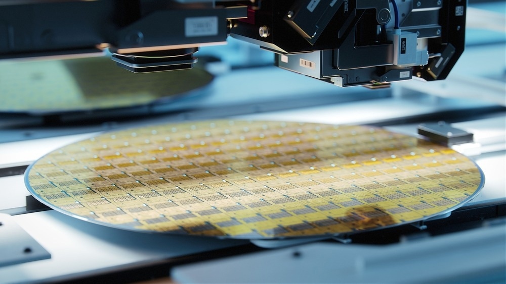
Image Credit: IM Imagery/Shutterstock.com
In this article, AZoNano explores what a semiconductor wafer is, covering its composition, manufacturing process, and the challenges faced in its fabrication.
Future development areas for semiconductor wafer fabrication will also be covered, as well as the efforts being made by researchers to make the semiconductor wafer cost-efficient.
What is a Semiconductor Wafer?
A semiconductor is a material that has properties that fall between those of an insulator and a conductor. It can be used to make a semiconductor wafer, thin slices of semiconductors made from crystalline silicon employed in manufacturing integrated circuits, and many renewable energy technologies.
A semiconductor wafer is circular and can have a diameter ranging from a few millimeters to centimeters. Other microelectronic devices can be built on and use the semiconductor wafer as a substrate.
Where is a Semiconductor Wafer Used?
A Semiconductor wafer is used in the manufacture of integrated circuits, microchips, solar cells, and photovoltaics. These form the foundation of modern electronic devices such as computer chips, smartphones, tablets, cars, cameras, and other devices that rely on semiconductors wafer technology.
Making a semiconductor wafer is very complex and requires very high precision and accuracy.
How to Make a Semiconductor Wafer
Making a semiconductor wafer is complex and requires a high level of precision.
The first step in making a semiconductor wafer is to extract silicon from sand. Silicon is the most abundant element on Earth, but it is not found in its pure form. The sand is first heated to a high temperature, which causes the silicon to melt. The molten silicon is then purified using a process called zone refining.
Once the silicon is purified, it is grown into a large, cylindrical ingot. This is done using the Czochralski method. A small piece of pure silicon is placed in a crucible of molten silicon. The crucible is then rotated, and the molten silicon is slowly pulled up into a cylindrical shape. The ingot is later cut into thin semiconductor wafers.
The semiconductor wafer is then polished to a mirror finish. This is done to remove any impurities on the surface. This is followed by subjecting the semiconductor wafer to a series of chemical treatments to make them more conductive.
The next step in making a semiconductor wafer is to deposit the desired semiconductor material onto the wafer. This is done through a process known as lithography. Lithography uses a light-sensitive chemical called photoresist to create a pattern on the wafer. The semiconductor wafer is then exposed to light, which hardens the photoresist in areas not covered by a mask. The unhardened photoresist is then washed away, leaving behind a pattern of exposed silicon.
The exposed semiconductor wafer is then implanted with dopants, which are atoms that give the silicon its desired electrical properties. The dopants are implanted using a process called ion implantation.
The semiconductor wafer is then subjected to a series of other processing steps, such as etching and oxidation. These steps create the desired features on the wafer, such as transistors and resistors.
The final step in making a semiconductor wafer is to test it to ensure it meets the desired specifications. When satisfactory, the semiconductor wafer is then packaged and shipped to a manufacturer.
Fabricating a Semiconductor Wafer: The Challenges
Semiconductor wafer manufacturing is a complex process requiring precision and adherence to strict standards. Understanding the intricacies involved in creating a semiconductor wafer enables us to appreciate its significance and anticipate advancements that will further enhance the quality and affordability of semiconductor wafers.
One of the biggest challenges is maintaining a clean environment during semiconductor wafer manufacturing. Even small amounts of contamination can ruin an entire batch of semiconductor wafers.
Another is the need for precise control of the semiconductor wafer manufacturing process to ensure high levels of precision and accuracy.
The tolerances required for semiconductor wafers are very tight, and any defects can lead to the failure of the device.
The Future of Semiconductor Wafer Synthesis
The future of semiconductor wafer synthesis looks promising. Increasing demand for semiconductor wafers, as well as research and development, drives the global semiconductor wafer market. To illustrate, the market is estimated to reach about $27.13 billion by 2030, growing at a CAGR of 4.8% during the 2021-2030.
Researchers are exploring new materials and manufacturing techniques that could lead to cheaper and better production methods.
For example, according to an article published in the ACS Nano Journal, scientists from the Nanyang Technological University, Singapore (NTU Singapore) and the Korea Institute of Machinery & Materials (KIMM) developed a method to design highly uniform and scalable semiconductor wafers, which can bring new opportunities for higher yields and semiconductor wafers that are cost-efficient.
In addition, in a recent Nature article, a strategy combining human expert design with optimization algorithms to improve semiconductor process efficiency was developed. Such processes can directly impact the cost-efficient production of semiconductor wafers.
Improving yields in semiconductor wafer fabrication depends heavily on in-line inspection systems. These systems are often deployed at every process step to ensure the traceability of every single semiconductor wafer at different stages of production.
These new technologies are expected to decrease the cost of semiconductor wafers, making them more accessible to a wider range of applications.
The Future of Semiconductor Wafers
A semiconductor wafer is a vital component in electronic devices, and its fabrication process requires precision and adherence to strict standards. Ongoing research and development efforts offer promising prospects for cost-effective production methods.
Collaborations between human expertise and optimization algorithms drive improvements in the semiconductor process efficiency, while in-line inspection systems enhance yields and traceability for semiconductor wafer manufacturing. These advancements are expected to decrease the cost of the semiconductor wafer, making it more accessible for various applications in the future.
References and Further Reading
Frost, O. (2021). The Trends Shaping Semiconductor Wafer Manufacturing [Online]. AZoM.com. Available at: https://www.azom.com/article.aspx?ArticleID=20380
Kanarik, K.J., Osowiecki, W.T., Lu, Y. (Joe), Talukder, D., Roschewsky, N., Park, S.N., Kamon, M., Fried, D.M., Gottscho, R.A. (2023). Human–machine collaboration for improving semiconductor process development. Nature 616, pp. 707–711. doi.org/10.1038/s41586-023-05773-7
Enuh, B.M. (2023). Presenting Novel Stable Ultrawide Bandgap Semiconductor Materials [Online], AZoM.com. Available at: https://www.azom.com/article.aspx?ArticleID=22575
Samsung. (2021). What is a wafer? [Online], Semiconductor.samsung.com. Available at: https://semiconductor.samsung.com/us/support/tools-resources/fabrication-process/eight-essential-semiconductor-fabrication-processes-part-1-what-is-a-wafer
Zhao, Z.-J., Shin, S.-H., Lee, S.Y., Son, B., Liao, Y., Hwang, S., Jeon, S., Kang, H., Kim, M., Jeong, J.-H. (2022). Direct Chemisorption-Assisted Nanotransfer Printing with Wafer-Scale Uniformity and Controllability. ACS Nano 16, pp. 378–385. doi.org/10.1021/acsnano.1c06781.
Disclaimer: The views expressed here are those of the author expressed in their private capacity and do not necessarily represent the views of AZoM.com Limited T/A AZoNetwork the owner and operator of this website. This disclaimer forms part of the Terms and conditions of use of this website.