Advancements in nanotechnology fabrication and characterization tools have facilitated a number of developments in the creation of new two-dimensional (2D) materials and gaining and understanding of their unique properties.
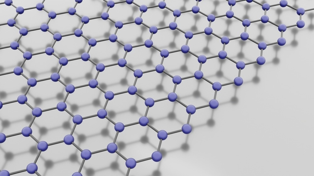
Image Credit: MZinchenko/Shutterstock.com
2D materials are characterized by their nanometer thickness in one dimension. Most 2D materials are only a single atomic layer in thickness and can be layered into more complex heterostructures to fine-tune particular properties of interest and create functional devices for use as sensors or transistors.1
In the other ‘long’ dimension of the material, a 2D material usually has a periodically repeating unit cell. The unit cell is composed of the atoms that make up the elemental composition of the sample and is the smallest repeating pattern that the whole material is composed of.
One of the earliest 2D materials to be discovered was graphene –composed purely of carbon.2 Graphene has generated a huge amount of interest as a material as many properties, such as its electrical conductivity, differ from the behavior of the bulk carbon samples. The unit cell of the sample consists of two carbon atoms, typically separated by 1.42 Å and a unit cell dimension of 2.46 Å.3
However, it is possible that defects can occur in the spatial arrangement of the atoms in the unit cell. Although defects may be small localized imperfections in a unit cell, the presence of defects in a sample can have a dramatic impact on the overall properties of the material. It is also possible if there are multiple defect sites in the material, to get defect-defect interactions.
Defects in 2D Materials
For some applications, intentionally introducing defects into 2D materials can be beneficial. There is currently a very active area of research into performing computational simulations to predict which sites and types of defects may lead to a desirable change in the material properties.4 This might include defects such as the creation of vacancies – such as missing atoms – at a certain point of the unit cell.
Advances in nanoscale fabrication methods have made it possible to selectively introduce such defects. Using techniques such as ion beams, it is possible to selectively displace atoms from the lattice and create local vacancies.5 Another possibility for controlling the properties of 2D materials is the introduction of dopants or intentionally engineering other defect types using other methods of sample irradiation.6 Such approaches have been used to create highly luminescent hexagonal boron nitride materials that could be used as room-temperature quantum emitters.
Characterizing Defects
Being able to create defects in 2D materials means there need to be techniques that can be used to characterize them. The challenge for characterization techniques for profiling defects needs to have a very high spatial resolution, as many defects are either the absence of a single atom or a small displacement of an atomic site within the lattice.
Electron microscopy methods excel in their high spatial resolutions. Electron microscopy methods are capable of achieving nanometer-scale spatial resolution and have been used extensively in the characterization of both 2D materials and heterostructures made from the materials.7
One of the main types of electron microscopy, transmission electron microscopy (TEM), can achieve sub-Angstrom and be used to image single atoms.8 TEM is therefore ideal for imaging defect sites as, as long as sufficient image contrast is achievable, it is possible to look at single atomic sites in the layers of the 2D materials.7
As well as being used to characterize defect sites, electron microscopy methods can be used to induce defects in 2D materials. For example, in molybdenum disulfide (MoS2), the electron impact energy of the incident electron beam that would be used for imaging can also introduce the defect sites.9 The formation of defects can lead to symmetry breaking in the local structure and changing the overall final properties of the material.
However, defect formation can be problematic for electron microscopy characterization of materials as, if this formation is unwanted, it is a type of damage mechanism that has altered the state of the original material. Reducing the intensity of the electron beam or working at energies below the knock-off thresholds can help reduce the sample damage, but minimization or elimination of sample damage has been one of the key challenges for imaging 2D materials and defects with electron microscopy methods.
Sometimes, alternative methods like scanning electron microscopy can provide another means of characterization with high spatial resolution. Still, the main breakthrough for mostly damage-free imaging has been the development of low-voltage aberration-corrected microscopes.10
Low-voltage methods are now also being used not just to capture static atomic arrangements in 2D materials but to image dynamic atomic motion in samples which can be used to image defect dynamics in materials such as semiconductors.10 Electron microscopy methods are very well-suited to imaging nanoscale structures and so likely to remain one of the main characterization techniques for 2D materials and their defects.
References and Further Reading
Wang, H., Liu, F., Fu, W., Fang, Z., Zhou, W., & Liu, Z. (2014). Two-dimensional heterostructures: fabrication, characterization, and application. Nanoscale, 6, pp. 12250–12272. https://pubs.rsc.org/en/content/articlelanding/2014/NR/C4NR03435J
Novoselov, K. S., Geim, A. K., Morozov, S. V., Jiang, D. E., Zhang, Y., Dubonos, S. V., ... & Firsov, A. A. (2004). Electric field effect in atomically thin carbon films. Science, 306(5696), pp. 666-669. https://www.science.org/doi/10.1126/science.1102896
Yang, G., Li, L., Lee, W. B., & Ng, M. C. (2018). Structure of graphene and its disorders : a review. Science and Technology of Advanced Materials, 19(1), pp. 613–648. https://www.tandfonline.com/doi/full/10.1080/14686996.2018.1494493
Ping, Y., & Smart, T. J. (2021). Computational design of quantum defects in two-dimensional materials. Nature Computational Science, 1, pp. 646–654. https://www.nature.com/articles/s43588-021-00140-w
Kretschmer, S., Ghaderzadeh, S., Facsko, S., & Krasheninnikov, A. V. (2022). Threshold Ion Energies for Creating Defects in 2D Materials from First-Principles Calculations: Chemical Interactions Are Important. The Journal of Physical Chemistry Letters, 13, pp. 514–519. https://pubs.acs.org/doi/10.1021/acs.jpclett.1c03995
Fischer, M., Caridad, J. M., Sajid, A., Ghaderzadeh, S., Gammelgaard, L., Bøggild, P., Thygesen, K. S., Krasheninnikov, A. V, Xiao, S., Wubs, M., & Stenger, N. (2021). Controlled generation of luminescent centers in hexagonal boron nitride by irradiation engineering. Science Advances, 7, p. eabe7138. https://www.science.org/doi/10.1126/sciadv.abe7138
Chang, Y., Han, H. N., & Kim, M. (2019). Analyzing the microstructure and related properties of 2D materials by transmission electron microscopy. Applied Microscopy, 49, p. 10. https://appmicro.springeropen.com/articles/10.1186/s42649-019-0013-5
Smith, D. J. (2008). Ultimate resolution in the electron microscope? Materials Today, 11, pp. 30–38. https://www.sciencedirect.com/science/article/pii/S1369702109700057
Kretschmer, S., Lehnert, T., Kaiser, U., & Krasheninnikov, A. V. (2020). Formation of Defects in Two-Dimensional MoS 2 in the Transmission Electron Microscope at Electron Energies below the Knock-on Threshold: The Role of Electronic Excitations. Nano Letters, 20, pp. 2865–2870. https://pubs.acs.org/doi/10.1021/acs.nanolett.0c00670
Graaf, S. De, Ahmadi, M., Lazic, I., Bosch, E. G. T., & Kooi, B. J. (2021). Imaging atomic motion of light elements in 2D materials with 30 kV electron microscopy. Nanoscale, 13, p. 20683. https://pubs.rsc.org/en/content/articlelanding/2021/NR/D1NR06614E
Disclaimer: The views expressed here are those of the author expressed in their private capacity and do not necessarily represent the views of AZoM.com Limited T/A AZoNetwork the owner and operator of this website. This disclaimer forms part of the Terms and conditions of use of this website.