The discovery of graphene ushered in a new age of materials science research: two-dimensional (2D) materials. This article will explain why we should stack 2D materials and how stacking allows us to uncover new features and uses.
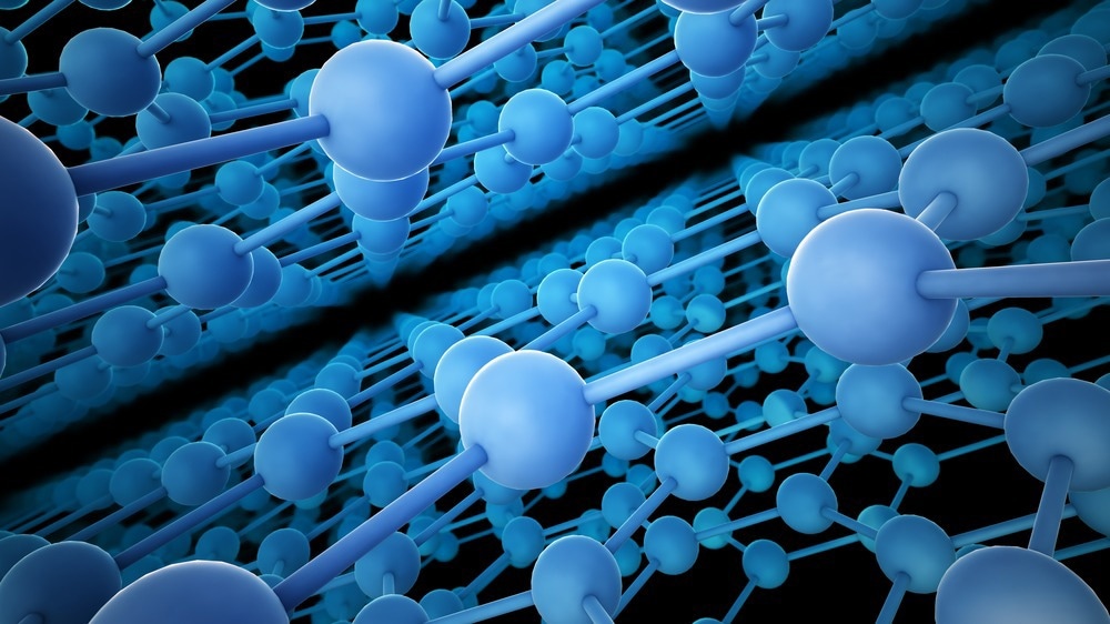
Image Credit: Mopic/Shutterstock.com
Over the last decade, there has been a surge in research concentrating on 2D materials other than graphene. Furthermore, by stacking different 2D materials, the attributes of 2D materials can be modified and enhanced.
What Are 2D Materials?
Two-dimensional (2D) materials are a type of nanomaterial that has one dimension that is only a few atomic layers thick (in nanometer scale) and two additional dimensions that are bigger than 100 nm, resembling a large but very thin sheet (like a piece of paper).
Researchers are particularly interested in 2D materials due to their distinct and extraordinary physical and chemical properties compared to their 3D bulk counterparts.
Outstanding electronic conductivity, high mechanical strength, and high surface area to volume ratio are among the most remarkable qualities of 2D materials, making them appealing for a wide range of applications.
2D materials, for example, are perfect for catalytic reactions due to their high surface area, while their superior electronic conductivity makes them suitable for application in electronics and energy storage systems. Furthermore, because of their thin and flat structure, 2D materials can be stacked or layered in various ways to create new materials with specific properties. Among the diverse range of 2D materials are graphene (conductors), transition metal dichalcogenides (TMDs), insulators hexagonal boron nitride (hBN), semiconductors made of only one element (silicene, phosphorene, germanene).
How Are 2D Materials Stacked?
The true potential of these two-dimensional layered materials may be revealed by their ability to be stacked layer by layer in any desired order to form unique three-dimensional (3D) architectures with whole new functionality. For example, a work published in PHYSICAL REVIEW B in 2007 predicted that when graphene was placed over hBN, it produced bandgap in graphene, leading to a paradigm shift in graphene electronics.
Stacking techniques are critical to improving device performance for various 2D material-based stacked architectures. Stacking can be achieved by liquid exfoliation, mechanical exfoliation, reduction-oxidation, chemical vapor deposition (CVD), epitaxial growth, and wet-chemical synthesis. The most often employed of these are mechanical exfoliation and CVD, which will be discussed below:
Top-Down Approach: Mechanical Transfer Process
The primary steps in the top-down approach are as follows.
Starting with a Si substrate, a water-soluble layer is firstly spin-coated, then a PMMA carrier. Following that, the appropriate top material (for example, graphene) is exfoliated onto the PMMA carrier.
The sample was then submerged in a water bath, and as the water-soluble polymer dissolved, the Si substrate fell to the bottom of the bath, leaving a floating layer on top. Then, the backside of the PMMA film is mounted to a glass transfer slide, and a graphene sheet is positioned on hBN flake using an optical microscope and a micromanipulator.
Finally, the PMMA film is removed after transfer by dissolving it in acetone. This technology has been widely used to create various vertically stacked 2D heterostructures, including Gr (graphene)/MoS2, Gr/WS2, and multilayered stacking heterostructures such as Gr/MoS2/h-BN, WSe2/MoS2.
Bottom-Up Approach: CVD
Although 2D vertical heterostructures can be created using a top-down approach, their practical applications are limited. To overcome this issue, the CVD technique has been most widely adopted.
In this technique, a reaction chamber is typically filled with one or more gaseous precursors. The gases chemically react with one another to produce solid materials that deposit on the surface of a heated solid substrate, resulting in the formation of equivalent 2D materials. For example, Peking University researchers recently reported the direct development of large-area graphene on hBN sheets utilizing an atmospheric pressure CVD technique with methane as the carbon precursor.
By altering the growth temperature, the CVD technique can create lateral heterostructures and vertical heterostructures. Researchers discovered that vertical and lateral WS2/MoS2 heterostructures could be produced at temperatures of 850 and 650 °C, respectively. The CVD technique not only yields large-area 2D material, but also allows for the direct growth of diverse stacking structures.
What Are the Benefits of Stacking 2D Materials?
Due to their high aspect ratio and extreme sensitivity to environmental changes, MoS2 is ideal for biosensing applications. However, MoS2 is sensitive to the presence of moisture and oxygen, which limits its applicability. Researchers found that a graphene/MoS2 heterostructure has a significant advantage in terms of stability and sensitivity.
In photovoltaics, the 2D heterostructure solar cell could produce efficiencies that are 1-3 orders of magnitude greater.
In photo-electronics, graphene has excellent electron mobility, but the zero gap nature of graphene may limit photoresponsivity. The direct band gap of monolayer TMD materials results in a high absorption coefficient, though it has poor mobility. As a result, researchers have attempted to combine these benefits by stacking graphene and TMD to improve light responses.
References and Further Reading
Bhimanapati, Ganesh R., et al. (2015). Recent advances in two-dimensional materials beyond graphene. ACS nano. doi/10.1021/acsnano.5b05556
Guo, Hao‐Wei, et al. (2021). Stacking of 2D materials. Advanced Functional Materials. doi.org/10.1002/adfm.202007810
Giovannetti, Gianluca, et al. (2007). Substrate-induced band gap in graphene on hexagonal boron nitride: Ab initio density functional calculations. Available at: https://journals.aps.org/prb/abstract/10.1103/PhysRevB.76.073103
Dean, Cory R., et al. (2010). Boron nitride substrates for high-quality graphene electronics. Nature nanotechnology. Available at: https://www.nature.com/articles/nnano.2010.172
Sun, Jingyu, et al. (2015). Direct chemical vapor deposition-derived graphene glasses targeting wide ranged applications. Nano letters. doi/full/10.1021/acs.nanolett.5b01936
Lim, Hyunseob, et al. (2014). Stacking of two-dimensional materials in lateral and vertical directions. Chemistry of Materials. doi/10.1021/cm502170q
Disclaimer: The views expressed here are those of the author expressed in their private capacity and do not necessarily represent the views of AZoM.com Limited T/A AZoNetwork the owner and operator of this website. This disclaimer forms part of the Terms and conditions of use of this website.