Discover the step-by-step process, unique advantages, and diverse applications of chemical vapor deposition (CVD) and delve into how this technique is revolutionizing the production of 2D materials.
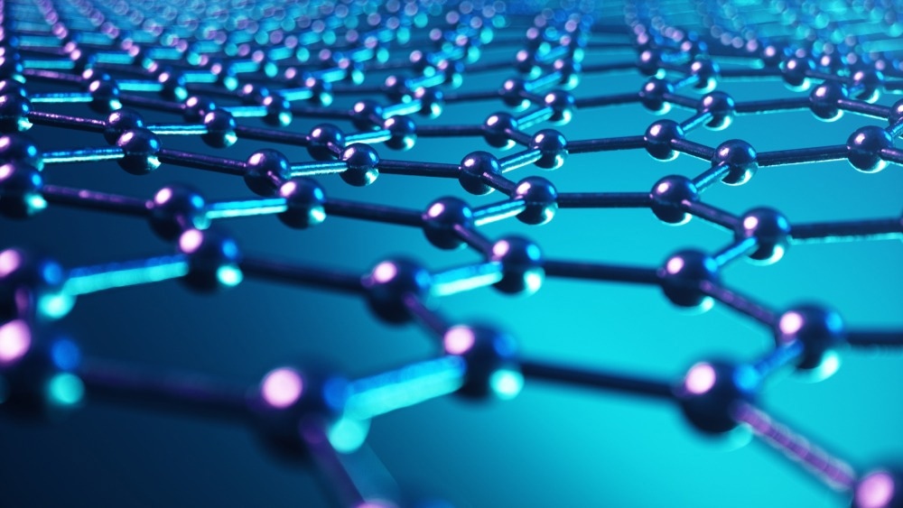
Image Credit: Rost9/Shutterstock.com
Two-dimensional (2D) materials have an atomic-scale thickness, which gives them exceptional capabilities. Graphene, likely the most well-known 2D material, has opened the door for others, each with distinct mechanical, electrical, and thermal properties, such as boron nitride, phosphorene, MXene, and transition metal dichalcogenides (TMDs). These materials provide breakthrough technological advancements in a variety of domains, including electronics, energy storage, and sensing.1
Why is Chemical Vapor Deposition (CVD) Used?
Two broad approaches can be used to manufacture 2D materials: bottom-up growth methods and top-down exfoliation procedures. Mechanical and liquid phase exfoliation is included in the former, and molecular assembly, atomic layer deposition, physical vapor deposition (PVD), vapor phase transport (VPT), and chemical vapor deposition (CVD) are included in the latter.2
Among the many techniques used to synthesize 2D materials, CVD is notable for its accuracy and scalability. CVD entails the chemical reaction of gaseous precursors to produce thin coatings onto a substrate. This process has several benefits over other methods, mainly because it can produce large-area, high-quality films with precise thickness.2
Step-By-Step Process in CVD
The fabrication of 2D materials via Chemical Vapor Deposition (CVD) follows a systematic process outlined in a step-by-step guide. Initially, the substrate, like a silicon wafer or metal foil, is meticulously prepared as the platform for subsequent 2D material deposition.
Precursor gases, critical for the desired material formation, are introduced into the reaction chamber. Thermal activation, achieved by heating the chamber, initiates chemical reactions crucial for the material's deposition onto the prepared substrate. Subsequently, growth and nucleation occur, setting the stage for controlled growth to achieve the desired thickness and quality. This precision ensures uniformity and reproducibility, which is crucial for both research and industrial applications.
The final step in the CVD process is cooling and annealing. After the growth phase, the material undergoes cooling and annealing processes. Cooling stabilizes the material, while annealing enhances its crystallinity and optimizes its overall properties. This step contributes to the refinement of the material's structure, ensuring it meets the desired specifications for various applications.2,3
Benefits of Using CVD for Layered 2D Material Fabrication
CVD stands out prominently as a superior method for fabricating layered 2D materials, primarily owing to its scalability, uniformity, thickness control, and integration potential.
CVD has great scalability, which enables the production of large-area films, making it well-suited for industrial applications. This scalability is crucial for meeting the demands of mass production and ensuring the practical applicability of 2D materials in various technological domains.4
Another advantage is uniformity in films produced through CVD, arising from the controlled deposition process that ensures consistent and reproducible results. This uniformity is crucial for ensuring the reliability of material properties, which holds significance in both research and industrial applications.
Additionally, CVD offers unique thickness control capabilities, enabling researchers to regulate the thickness of the deposited 2D material precisely. This precise control is pivotal for tailoring the material's properties to meet specific application requirements, enhancing its versatility and adaptability across various industries.2
One of the standout advantages is the integration Potential offered by CVD. This method seamlessly integrates 2D materials into existing semiconductor fabrication processes. This integration capability is a game-changer, enabling the smooth incorporation of 2D materials into electronic devices.
CVD's compatibility with established manufacturing processes ensures that 2D materials can be readily assimilated, opening up new possibilities for enhancing the performance of electronic components.4,5
Examples of 2D Materials Fabricated Through CVD
The effectiveness of CVD in fabricating various 2D materials with customized properties is demonstrated by several noteworthy examples. In the first instance, Graphene Growth on Copper Substrates, researchers harnessed CVD to cultivate high-quality graphene layers on copper substrates. The resultant graphene exhibited remarkable electrical conductivity and mechanical strength, effectively showcasing the scalability of CVD in producing graphene on an industrial scale.6
In transition metal dichalcogenides, molybdenum disulfide (MoS2) synthesis involves using CVD to synthesize monolayer MoS2 films with precise control over thickness. The resulting material showcased exceptional electronic and optical properties, underscoring the precision achievable through CVD in synthesizing intricate 2D materials.7
Moving on to dielectric applications, hexagonal boron nitride (hBN) for electronics utilized CVD to deposit hBN layers with controlled thickness on various substrates. The resulting hBN films exhibited excellent dielectric properties, rendering them suitable for electronic applications. This study vividly illustrated the versatility of CVD in fabricating a spectrum of 2D materials to meet diverse technological needs.8
Lastly, in exploring emerging 2D materials, researchers successfully utilized CVD to synthesize black phosphorus with controlled layer thickness. The resulting material displayed unique anisotropic electrical and thermal properties, highlighting the adaptability of CVD for the fabrication of novel and advanced 2D materials. These instances collectively emphasize the versatility, precision, and scalability of CVD as a powerful tool in synthesizing a wide array of 2D materials for various applications.9
Conclusion
CVD has established itself as a powerful technique for fabricating 2D materials layer by layer. Its scalability, precision, and versatility make it a preferred method in the quest for harnessing the unique properties of these materials.
Through the discussed examples, it is evident that CVD not only enables the production of high-quality films but also opens avenues for integrating 2D materials into various technological applications, promising a future where these atom-thin wonders play a pivotal role in shaping the landscape of advanced materials and electronics.
References and Further Reading
Zhang, Y., et al. (2013). Review of Chemical Vapor Deposition of Graphene and Related Applications. Accounts of Chemical Research, 46, pp.2329–2339.
Cai, Z., et al. (2018). Chemical Vapor Deposition Growth and Applications of Two-Dimensional Materials and Their Heterostructures. Chemical Reviews, 118, pp.6091–6133.
Alam, S., et al. (2021). Synthesis of emerging two-dimensional (2D) materials – Advances, challenges and prospects. FlatChem, 30, p.100305.
Seravalli, L. & Bosi, M. (2021). A review on chemical vapour deposition of two-dimensional MOS2 flakes. Materials (Basel), p.14.
Zeng, M. & Fu, L. (2018). Controllable Fabrication of Graphene and Related Two-Dimensional Materials on Liquid Metals via Chemical Vapor Deposition. Accounts of Chemical Research, 51, pp.2839–2847.
Ibrahim, A., et al. (2015). Effects of annealing on copper substrate surface morphology and graphene growth by chemical vapor deposition. Carbon N. Y., 94, pp.369–377.
Singh, A., et al. (2019). Effect of different precursors on CVD growth of molybdenum disulfide. Journal of Alloys and Compounds, 782, pp.772–779.
Orofeo, C. M., et al. (2014). Ultrathin Chemical Vapor Deposition (CVD)-Grown Hexagonal Boron Nitride as a High-Quality Dielectric for Tunneling Devices on Rigid and Flexible Substrates. The Journal of Physical Chemistry. C, 118, pp.3340–3346.
Smith, J. B., et al. (2016). Growth of 2D black phosphorus film from chemical vapor deposition. Nanotechnology, 27, p.215602.
Disclaimer: The views expressed here are those of the author expressed in their private capacity and do not necessarily represent the views of AZoM.com Limited T/A AZoNetwork the owner and operator of this website. This disclaimer forms part of the Terms and conditions of use of this website.