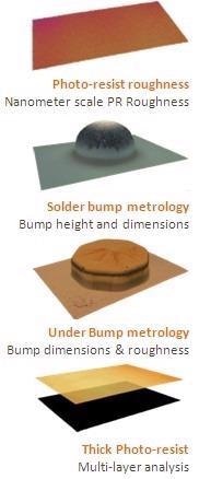
The Zeta™-388 is a fully automated wafer metrology system that can handle 100mm, 150mm, and 200mm wafers. The system is designed for applications such as bump height, etch depth, roughness, film thickness, and wafer bow. Based on KLA Instruments’ revolutionary Multi-Mode measurement approach, the Zeta-388 optical profiler packs the power of five separate measurement tools into a single compact platform.
Simple
The Zeta-388 3D software has a simple and intuitive user interface for data acquisition and analysis. A short learning curve for engineers and operators results in better productivity.
Versatile and Fast
The high resolution 3D optical profiler requires less than 30 seconds per ZDot™ structured illumination measurement. Zeta Multi-Mode capability means that bump height, film thickness, roughness, and wafer bow can be measured without the need for unloading the wafer and transferring it to a new tool.
Fab Ready
The Zeta-388 meets Class 100 standards and can be equipped with a multi form-factor handler with pre-aligner. The comprehensive KLA 3D software, including SECS/GEM, completes the fab-ready package.
Multi-Mode Optics for Any Type of Measurement
The Zeta-388 is available with multiple advanced imaging methods:
- ZDot™ structured illumination 3D measurement is the measurement technique standard on all Zeta optical profilers. ZDot™ technology enables True Color measurement with a 13nm step resolution.
- PSI phase shifting interferometry provides nanometer-level step height measurements, even over a 4.5mm field of view
- VSI vertical scanning interferometry offers Angstrom-level step height measurements over a large field of view
- ZFT
spectroscopic reflectometry maps the thickness of transparent thin films across the wafer
Image Credit: KLA Instruments™
Shorter Process Feedback Cycle
The Zeta-388 also includes high quality camera and optics to enable automated defect inspection by mapping defects across the sample. The high resolution 3D surface analysis measurements from the Zeta-388 profilers provide insight for most defects and process excursions, and decrease the number of wafers or sites that need to be reviewed by time-consuming and costly SEM or AFM. The Zeta-388 is capable of measuring from nanometers up to millimeters.
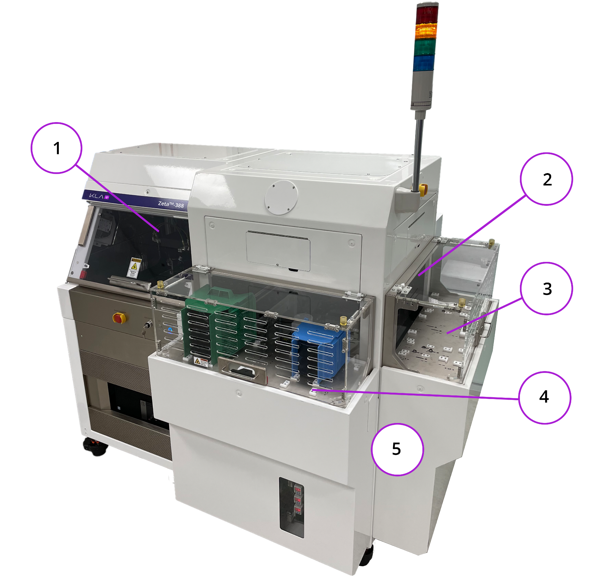
Image Credit: KLA Instruments™
- Zeta3D™ measurement head - Configure the tool with various illumination and magnification options
- Flat or notch finder - Dedicated flat or notch finder for each measurement head
- Cassette mapper - Individual cassette mapper on each port to allow proper wafer transfer as well as sorting and binning
- Multi-form factor - Choose two different wafer sizes to enable multi-form factor functionality without having to change hardware
- Precision motion and compact handler design
System Features
- Camera: Color CCD camera
- Illumination: Dual white light LEDs for ZDot and TrueColor; Green LED for PSI; Nomarski for differential contrast, white back light LED for through-sample illumination
- Magnification: 35,000X combined optical and digital
- Z travel: 40mm (standard), 200µm (piezo)
- Motorized stage: Up to 200mm x 200mm XY travel
- Vibration isolation: Built-in
- Wafer size: 100mm, 150mm, 200mm
- Workstation PC: 16GB/32GB RAM, 1TB HDD
- Cassette stations: 1-4; each station can support two sizes
Full Wafer Mapping
The Zeta software’s automated wafer deskew and pattern matching capability can be used to set up a multi-site sequence using ZFT. Typical nine-site and 49-site maps can be easily created and executed. Data is stored in *.csv or text format for easy export.
Wafer Bow and Film Stress
Semiconductor fabs have normally relied on a line scan method to measure 2D bow of wafers, either laser-based or using a stylus profiler. Using the Zeta-388 optical profiler, the process engineer can program an array of measurements across the wafer to obtain the total 3D wafer warp profile. Pre- and post-film deposition measurements are used to measure the film stress.