|
• AIST has obtained results which reverse the conventional wisdom that superconducting films formed by processes needing a vacuum atmosphere are of high performance but expensive, while superconducting thin films produced by solution processes are inexpensive but of low performance.
• They achieved a critical current density, an important index for superconducting film performance, of six million A/cm2, which corresponds to the world's highest level performance, and is comparable to or more than those of thin films produced using vacuum processes.
• AIST has enabled a reduction in film production costs to less than one tenth of those for vacuum processes. Our technique has further enabled high-speed production of not only superconducting thin films but also various large-area functional thin films.
Synopsis
Mitsugu Sohma and Tetsuo Tsuchiya (Senior Researchers) et al. of the Advanced Manufacturing Research Institute (Hideto Mitome, Director) of the National Institute of Advanced Industrial Science and Technology (AIST; Yoshikawa Hiroyuki, President), jointly with Kunihiko Koyanagi (Researcher) and Takashi Ebisawa (Senior Researcher) of the Department of Research and Development (Tadao Iwadate, General Manager and Executive Director) of the Japan Steel Works, Ltd. (JSW; Masahisa Nagata, CEO), have established a low-cost, high-speed production technique of high-performance thin films by combining a solution process with a laser irradiation technique.
Various metallic oxide thin films have been used for devices such as solar cells, displays, sensors, capacitors, and so on. These functional thin films have been mainly produced using processes which need an expensive vacuum atmosphere. On the other hand, solution processes enable a reduction in the production costs, because the films can be produced in air. However, thin films formed using solution processes have not had sufficient performance.
In this work, by combining a production technique for oxide superconductors (YBa2Cu3O7: YBCO) using a metalorganic deposition (MOD) method, which is one of the solution processes AIST has developed, with an excimer-laser annealing technique developed by JSW, the researchers have succeeded in the improvement of their characteristics and the enhancement of production process efficiency (Figure 1).
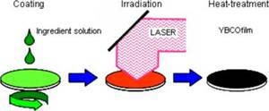
Figure 1. High-speed film formation technique consisting of a solution coating process and a laser irradiation process
Using this method, they have succeeded in an enhancement of film production speed to five times that using conventional solution processes. In the production of epitaxial thin films we have achieved critical current densities, an important index of super-conduction, of six million A/cm2 (Figure 2), a value of the world's highest class. This value is comparable to or greater than those of superconducting thin films produced by vacuum processes.
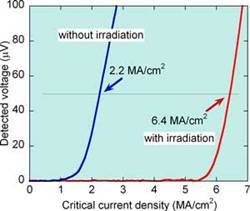
Figure 2. Performance gain by laser irradiation
This method enables the cost reduction and mass production of thin film devices, long tapes etc., by simultaneous patterning with masks (Figure 3) and by continuous film formation with moving substrates. Thereby, the film production cost can be reduced to less than one tenth of those formed using vacuum processes.
Figure 3. Patterned YBCO superconducting thin film. Black-patterned parts exhibit super-conduction.
The results enable not only a reduction in electric power transportation loss, which results in energy saving, the stabilization of electric power systems, which leads to safety and reassurance, and the enhancement in quality and sensitivity of mobile communications, but also the high-speed production of functional thin films.
Background and History of Research Work
Solar cells, which can contribute to energy saving and safety, displays, sensors, capacitors, etc., use various metallic oxides, which can exhibit transparent conductivity, magnetization, dielectricity, superconductivity, and optical functionality. However, to make devices from these functional materials, they must usually be formed into thin films. In particular, when the films are epitaxial ones, high performance can be obtained, enabling the creation of high-efficiency and innovative devices.
Until now, the production of high-quality epitaxial thin films has been carried out using gas-phase methods which need a high vacuum atmosphere, thus leading to high production cost; in particular, the methods are unfavorable to applications requiring large areas and long shapes.
On the other hand, solution processes are inexpensive methods because they do not use a vacuum, and are applicable to films with large areas and complicated forms. However, epitaxial thin films made by solution processes have not had sufficient performance. Until now, it has been accepted wisdom that thin films formed by vacuum processes are of high performance but expensive, while thin films made by solution processes in the air are inexpensive but of low performance.
Details of Research Work
Up to now, AIST has developed MOD methods for the formation of thin films using solutions without fluorine. In this work, by combining this method with an excimer-laser annealing technique by JSW (Figure 4), a production process has been developed for high-performance superconducting thin films in the air.
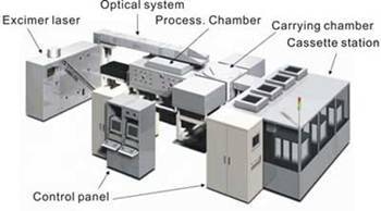
Figure 4. Overview of excimer laser
Using this new process (Figure 1), the researchers have formed YBCO superconductors of approximately 100 nm in thickness on substrates of an aluminum oxide single crystal with an interlayer. By an induction current method, the superconductors have been detected to exhibit a critical current density or an important index for super-conduction performance, at highest, over six millions A/cm2 at the liquid nitrogen temperature, which corresponds to approximately 3 times current densities previously obtained by conventional MOD methods (Figure 2). Also, this critical value is comparable to or more than those of superconducting thin films formed by vacuum processes, indicating that the performance of the superconducting thin films has achieved the world's highest level.
The low-cost superconducting thin films formed can be widely used as coated conductors for low-loss transportation of electric energy, thus resulting in energy saving, fault current limiters for stable and safe electric power systems, microwave devices for high-quality and high -sensitivity mobile communications etc.
Significant results obtained may be due to the fact that specific chemical bonds in the coating films are cut more effectively by laser-irradiation processing after coating than by conventional MOD methods with purely thermal energy, leading to the formation of good-quality precursors in which components including several metallic elements are homogeneously dispersed at the molecular level (Figure 5).
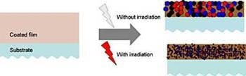
Figure 5. Schematic illustrations of the state of precursors. In the laser irradiation part the good-quality precursors with no compositional modulation can be formed.
Thus, this method enables shortening of the thermal treatment time needed for the synthesis of superconducting thin films from these metallic components, and also enables a reduction in the thermal treatment process temperature. Furthermore, because of the production of the good-quality precursors, partial composition variations hardly ever occur, and thus the impurity formation is suppressed, resulting in dramatic enhancement of super-conduction characteristics.
The film formation speed of the new method is approximately five times those of conventional coating-pyrolysis methods. In addition, this method enables continuous film formation on large area or long substrates by the expansion of laser-irradiation areas with mirrors or by continuous moving of substrates, respectively. Moreover, without complicated lithography processes but purely with simple photo masks, our method enables film formation and patterning at the same time (Figure 3).
In the future, the film production cost will be reduced to less than one tenth of those for the films formed by present vacuum processes. Furthermore, the authors think that the new method enables low-cost and high-speed production of not only superconducting thin films but also various large-area functional thin films.
Future Prospects
Hereafter, JSW plans to further advance technology development for large-area and massive production of superconducting thin films, and supply samples to users. In particular, applications to current limiters for stable electric power systems, microwave filters and antennas using simultaneous patterning for mobile communication base stations, etc. will be considered.
Moreover, JSW, adopting "materials and mechatronics" as its slogan, will consider not only the production of thin film materials but also the sales market for thin film production equipments utilizing excimer laser annealing techniques.
|