An interview with Dr Sam Marks, outlining the in situ abilities of Oxford Instruments TEM products, conducted by Alina Shrourou, BSc.
Please outline the challenges researchers face when analyzing nanostructures.
The main challenges when analyzing nanostructures come down to your sensitivity and your accuracy. With nanostructures especially, you can be looking at trace amounts of material and you want to be able to capture what's truly there. If you're analyzing down to individual atoms, you want to make sure that you are fully capturing that single atom, of Sulfur, for example.
Say you do capture that successfully; your second challenge is the accuracy. With EDS, it's very common for us to look at the full composition of a material from its spectra and measure its atomic percentage composition or its weight composition. It's all about being confident that our results are a true representation of the sample that you're analyzing.
There has recently been some real advances in dynamic in situ experiments, where you can use an in situ holder to effectively induce an atmosphere around your sample. This means that you can heat the sample up, or conduct experiments involving liquids, gases, or even electrical biasing, all in situ.
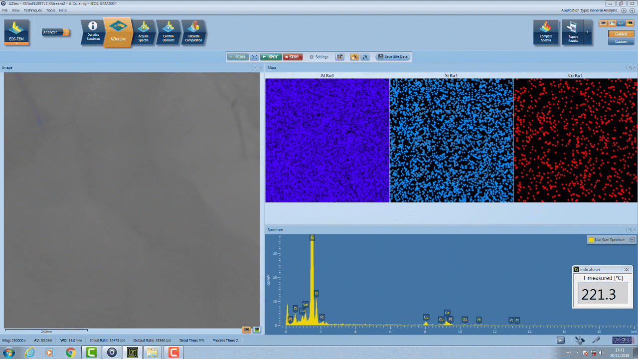
FIB lamella showing Al2Cu precipitation and annealing when heated from 0 - 450°C. (Sequence sped up 20x)
As this is becoming a more prominent form of analysis within TEM, we want to be able to do complimentary EDS at the same time. So, while you're running a heating experiment and seeing these chemical changes, we want to be able to map your sample and show you the chemical changes as they occur, which is quite challenging.
How can real-time feedback of in situ chemistry experiments enhance TEM observations?
In situ experiments essentially involves putting your lab inside the microscope in order to observe a chemical reaction. Currently, if you wanted to do EDS of your sample, you would need to pause that reaction and potentially lower the temperature if you were doing a heating experiment, so that you can acquire your EDS.
However, this artificially alters the experiment. If the reaction was occurring naturally, it wouldn't rise up to a temperature, stop (while you acquire your EDS) and then start to rise again. It's not a continuous experiment as you are changing the variables, resulting in invalid results.
The ability to observe these reactions in real time gives you a much truer representation of what's happening. It also captures smaller details that occur which you might not usually acknowledge. When you acquire a single map, you're only capturing a moment in time; whereas, if we can do this in real time, you get to see the full live experiment and see how it's evolving.
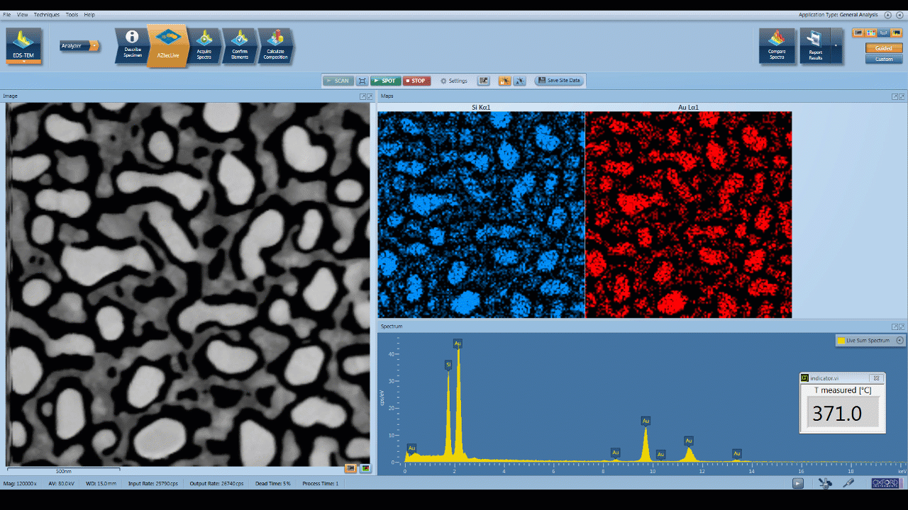
10 nm Au film on SiN membrane heated from 0 - 800°C showing particle agglomeration. (Sequence sped up 20x)
How is AZtecTEM optimised to allow easy nano-analysis for in situ experiments?
The first way that we have optimized AZtecTEM is within our detectors themselves. All of our detectors have optimized geometry. Everything is arranged to maximize the number of X-rays that are going from your sample to our detectors, whilst minimizing all the background X-rays which are always generated within a microscope.
 AZtecTEM: The most powerful solution for EDS in the TEM
Additionally, we also try and get the detectors as close to the sample as possible to maximise the solid angle. Solid angle is a measure of the X-ray exposure on the detector based on the geometry of the detector size and distance from sample. The closer you can get your detector to the sample, the larger the solid angle. We want that to be as large as possible, as this increases the efficiency and the number of X-rays that the detector sees.
Something which has optimized the AZtecTEM for heating experiments, is the integration with our Extreme electronics. If you are heating your sample up say, 1000 degrees, it will start releasing visible IR and UV radiation. IR and UV is electromagnetic radiation just like X-rays, so it is visible on the X-ray detector. It appears as really low energy noise, but it's much more dominant than your actual X-rays from your sample. In our previous generation detectors, the background radiation would become too great at ~700ﹾC, meaning that the detector would become saturated and stop working. The increased processing power of our Extreme electronics now allows us to continue collecting X-rays at temperatures greater than 1000ﹾC without saturating the detector.
What features make Ultim® Max unique compared to other silicon drift detectors?
The ability to process X-rays faster and at much higher throughput due to our Extreme electronics is very much one of our unique factors. It allows us to acquire all the background radiation but still have the ability to acquire the smaller quantity of X-rays that are coming from the samples.
.png)
Traditional semiconductor devices can only handle a certain number of inputs at a time, and they effectively have to turn themselves off while they're processing those inputs – this is known as “dead time”. We can process a lot more counts before our detectors have to turn themselves off, meaning that the Ultim® Max has a lower dead time and can undertake experiments in less time compared to other SDD’s.
How does AZtecTEM complement the Ultim® Max detectors for TEM?
AZtecTEM powers our Ultim Max range through the our powerful analyse platform, two new features that complement the Ultim max detectors are AZtecLive and M2T. AZtecTEM provides real time EDS mapping, allowing users to analyze experiments in real time. M²T is an advanced quantification process; It’s a key feature as it can measure the thickness of a sample; something novel to be able to do within the TEM.
We’re able to measure sample thickness because we can measure the quality of the electron beam inside the TEM. That is only made possible by understanding the quality of our detectors.
What types of applications can an increase in detector speed allow for EDS in the TEM?
The key thing here is the extra abilities and improvements our detectors provide for everyday EDS experiments in the TEM. Everything can be acquired in less time, to the same amount of accuracy. It gives you a great turnaround on samples and on your analysis, key for beam sensitive materials, time sensitive applications or high throughput industries; for example, semiconductor analysis where you might want to analyze a large number of samples in a small amount of time.
Although not relating to the increase in detector speed, M²T and our novel ability to measure the thickness of samples is something that we think could transform EDS in the TEM. Our results show a high level of accuracy for thickness measurement where other methods have a much higher associated error. M²T is a much more affordable and accurate method for measuring sample thickness, which can be important with any form of nanostructure.
.png)
Specimen thickness measurements acquired using M2T across the highlighted region on a FIB lamella.
How do you think the new range of detection offered by Oxford Instruments Nanoanalysis will advance elemental analysis?
It's the power and speed that comes in through the combination of our new detectors, their electronics and the software applications.
With M²T and advanced quantification, we are much more accurate and provide a higher level of confidence when analysing a samples chemical composition. Previously this has been a somewhat, speculative calculation, with high amounts of error associated to the quantification results. This, previously, was something very normal as it’s extremely difficult to exactly characterize the composition of a sample.
As we can characterize the electron beam with M²T, it gives us much more confidence in our results. This reduces the amount of error in our quantification, so that you have a much more accurate measurement, which is key for elemental analysis. Then of course we have the ability to conduct all of this in situ, and when combined with AZtecLive you can see what is truly there.
About Sam Marks
.jpg)
Dr Sam Marks graduated with a doctorate in Physics. He joined Oxford Instruments in 2018 and has always worked with a strong focus on electron microscopy. Sam has focused his research on S/TEM, in particular in-situ characterisation. He is currently working as a TEM Product Manager within the EDS Product Marketing Group.
Disclaimer: The views expressed here are those of the interviewee and do not necessarily represent the views of AZoM.com Limited (T/A) AZoNetwork, the owner and operator of this website. This disclaimer forms part of the Terms and Conditions of use of this website.