Photolithography is a fundamental fabrication process with a wide range of industrial applications, from manufacturing microelectronics and micro-electromechanical components to thin film patterning for biosensors. But how does it work?
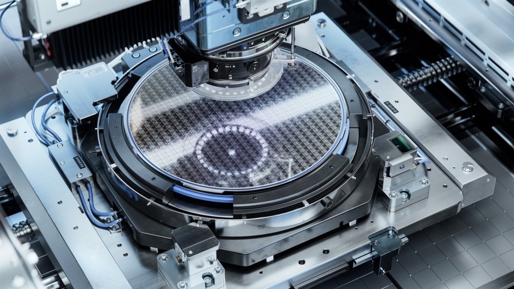
Image Credit: PastryShop/Shutterstock.com
Photolithography uses ultraviolet (UV) light to create complex geometric shapes and patterns onto a light-sensitive photoresist coating, transferring them to the underlying substrate. This article explores the basics of the technique, breaking down each key step involved.
Basics of the Photolithography Process
Photolithography involves the selective exposure of a photosensitive material to light, using a UV light source and a collimating optical system to create an image of a patterned mask onto a substrate coated with a photosensitive polymer layer (photoresist). This illuminated pattern is then transferred onto the substrate via a subsequent etching step.
In most photolithographic applications, thin silicon wafers, with their excellent thermal conductivity, are used as substrates. The entire process is made up of several steps that are executed sequentially at specific conditions and for a certain duration, depending on the desired outcome of the patterning process.
Photolithography works best on flat substrates, and the process is unsuitable for patterning high-curvature surfaces and creating complex 3D structures. Other, softer lithographic techniques are typically used to pattern curved or spherical surfaces.
The $200M Machine that Prints Microchips: The EUV Photolithography System
Video Credit: Branch Education/Youtube.com
Key Steps in Photolithography
When manufacturing a surface via photolithography, there are five fundamental processes involved: substrate preparation, photoresist application, soft baking, mask alignment and pattern exposure, and post-exposure baking and pattern transfer (etching or replica molding).
Substrate Preparation
A silicon wafer substrate is first baked at elevated temperatures (200-400°C) for 30-60 minutes to evaporate any water present, clearing the surface of unwanted hydroxyl molecules. Next, particulate matter and traces of organic, ionic, and metallic impurities are removed from the wafer surface. The cleaning process depends on the physical and chemical properties of the substrate materials, and can involve wet cleaning (a chemical bath) or dry-cleaning steps (plasma cleaning or UV irradiation).
Preparing the substrate in this way provides a clean, highly adhesive surface for the photoresist coating. Depending on the type of substrate and photoresist, a barrier layer (usually silicon dioxide) or adhesion promoter might be deposited on the cleaned wafer surface.
Photoresist Coating
A uniform layer of photoresist is then applied to the wafer surface. Most industrial photolithographic processes employ the spin coating technique, where the substrate rapidly rotates. Spin coating applies a centrifugal force to the surface, evenly spreading the photoresist solution across the substrate. The solvent evaporates, forming a uniform thin photoresist layer (0.1-10 μm in thickness).
Two types of photoresists can be used to transfer the pattern onto the substrate. When using a positive-tone photoresist, the exposed region of the photoresist becomes soluble to the photoresist developer. This type of photoresist enables higher spatial resolution and better control of the sidewall roughness of the patterned structures.
In contrast, upon exposure to light, a negative-tone photoresist crosslinks and becomes insoluble during the development step. This type of photoresist is most often used when high-aspect-ratio features and thick resist layers are required.
Soft Baking
Most of the solvent is removed from the photoresist during the soft baking step. This step is very important as it renders the resist layer photosensitive.
Positive resists might be incompletely exposed if a significant amount of residual solvent is present in the coating. Under-baked positive resists can be attacked by the developer in both exposed and unexposed areas, degrading the etching resistance of the exposed resist. Overbaking at this stage can degrade the photosensitivity of the resist by damaging the photosensitizer molecules in the resist layer.
Photomask Alignment and Pattern Exposure
Typically, the photomask is a quartz or glass plate patterned with the desired features, usually with a metal (chromium or molybdenum) coating. The mask can have a repeating pattern that covers the entire wafer, thus creating a large number of identical patterns (or dies), or cover a small portion of the wafer and create just a few dies (such masks are known as reticles).
The mask or reticle must be aligned and locked into the photolithographic equipment. When a reticle is used, it is translated stepwise parallel to the wafer surface, exposing a small portion of the wafer with each step. This is done using a 'stepper'.
The mask pattern can be transferred through direct contact, proximity, or projection exposure.
In direct contact, the mask is placed directly onto the photoresist surface, resulting in high spatial resolution. However, this technique increases the risk of mask damage and reduces the process throughput.
Proximity exposure keeps the mask a short distance from the photoresist, resulting in lower spatial resolution. In projection exposure, an optical system forms a scaled-down image of the mask onto the resist surface.
Modern photolithographic processes employ catadioptric projection optics, consisting of both refractive (lenses) and reflective (mirrors) elements, together with deep-UV (193 nm) or extreme-UV (13.5 nm) light sources to produce pattern features with characteristic dimensions of less than ten nanometers.
Development follows exposure, dissolving the unwanted areas of the photoresist using a developer (a combination of solvents, such as tetramethylammonium hydroxide and surfactants).
The duration of the development process is critical, as underdeveloped resist could prevent access to the underlying substrate by leaving a residual resist layer on the wafer. Conversely, an overdeveloped resist can distort the pattern transferred to the wafer. The wafer is rinsed with deionized water and spin-dried once development is complete.
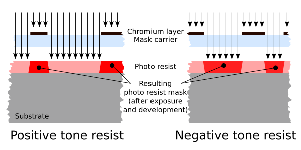 Image Credit: Cepheiden/Shutterstock.com
Post-Exposure Baking and Pattern Transfer
Finally, the photoresist is subjected to a baking process to harden and strengthen the remaining resist material to withstand the following pattern transfer steps without feature degradation. At this point, the photolithographic process is complete, and the wafer is ready for wet or dry etching, selective metal deposition, ion implantation, or used for replica molding.
Continue Reading: Using SEM to analyze surfaces post-production!
References and Further Reading
- M. Madou, C. Wang (2012). Photolithography. In: Bhushan, B. (eds) Encyclopedia of Nanotechnology. Springer, Dordrecht. Available at: https://doi.org/10.1007/978-90-481-9751-4_342
- Naulleau, P. (2019) Optical Lithography, In: Andrews, D. L., Lipson, R. H., Nann, T. (eds.) Comprehensive Nanoscience and Nanotechnology (Second Edition), Academic Press, 387-398. Available at: https://doi.org/10.1016/B978-0-12-803581-8.10433-3
Disclaimer: The views expressed here are those of the author expressed in their private capacity and do not necessarily represent the views of AZoM.com Limited T/A AZoNetwork the owner and operator of this website. This disclaimer forms part of the Terms and conditions of use of this website.