Silicon Carbide (SiC) has become one of the efficient replacement materials for silicon for various applications due to its unique properties that can be tunable through impurity doping and synthesis of different nanostructures.
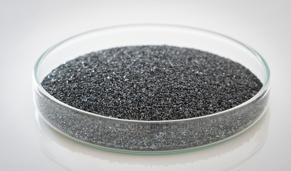
Image Credit: luchschenF/Shutterstock.com
Semiconductors are a vital part of electronic devices due to their conditional conductivity, which can be controlled through various parameters. Silicon carbide is a semiconducting compound made up of silicon and carbide, which forms a wide bandgap material.
Si and C are bonded to each other through strong tetrahedral covalent bonds formed by the sharing of electron pairs in sp3 hybridization. The resulting SiC has many unique properties with a variety of applications possible.
Polytypes of SiC
The Si-C planes could be stacked in different stacking orders to form different unit cell structures, giving rise to different polytypes of SiC. A few of the different lattices possible are 3C-Zinc blend, 2H-Wurtize, 4H-SiC, 6H-SiC and so on. With the variation in the unit cell, the number of atoms per unit cell also varies, which effects the number of energy bands and vibrational branches for a polytype.
With the variation in the unit cell, its physical as well as chemical properties also change. Another possible reason for the change in properties could be the change in the number of active donor and acceptor sites.
The two polytypes of great interest are the 4H and 6H-SiC, as the 4H and 6H active sites differ with two and three, respectively, for substituting the impurity elements. Its structure imparts many important properties to the SiC, making it suitable for applications requiring superior thermal conductivity, thermal stability, low thermal expansion, low switching losses and high chemical stability 1.
Doping of SiC
Compared with other wide bandgap semiconductor materials, p- and n- doping for a wide dopant concentration from 1014 to 1020 cm-3, is easily possible with SiC through in-situ doping or ion implantation.
SiC is mostly doped with donor-type impurities (nitrogen and phosphorous) and acceptor-type impurities (aluminum, boron and gallium) for increasing their electrical conductivity. Nitrogen substitutes the C in the SiC lattice, while phosphorous, aluminum and boron substitutes the silicon in the SiC lattice. The lattice parameter of the SiC changes with the doping density, dopant and the temperature of crystal formation.
On doping with nitrogen, lattice contraction, whereas on doping with aluminum, lattice expansion is reported; the stress in the lattice due to doping-induced lattice mismatch is crucial at the time of heterostructure formation during device fabrication 1,2,3.
How Are SiC Nanomaterials Synthesized?
SiC nanomaterials could be synthesized in different structures of 0D (solid nanocrystals, hollow nanospheres and core-shell spheres), 1D (Nanowires, nanotubes and core-shell nanocables), 2D and 3D nanostructures (nanowire flowers, hierarchical nanoarchitectures, tetrapods and so on).
Wet-chemical synthesis, pyrolysis, laser ablation, template-assisted vapor-solid method, chemical vapor deposition (CVD), vapor-liquid-solid mechanism, vapor-liquid mechanism, physical vapor deposition techniques and so on are employed for the synthesis of different structured SiC nanomaterials 4.
Properties of SiC
All the polytypes of SiC have wide optical indirect bandgap. The bandgap varies from approximately 2.4 to 3.35 eV from 3C to 2H, respectively. Due to having an indirect bandgap, SiC applications in electro-optical devices are limited; however, its applications in power electronics is vivid.
SiC crystals of reasonable quality is available in large areas for device fabrication. Optical and electronic properties vary for different polytypes and could be utilized in a wide range of applications.
4H-SiC is the most suitable polytype for applications in power electronics due to its high electron mobility, high critical electric field strength and availability of single-crystal wafers. These electronic properties are low for 6H-SiC and too low for 3C-SiC.
At room temperature, SiC has extremely low intrinsic carrier density, being 5 x 10⁻⁹ cm-3, compared to that of Si of 1 x 1010 cm-3, which makes SiC suitable for high temperature electronic applications. Moreover, the leakage current in SiC is very low due to the tolerance of SiC devices against defects.
This property, along with the high temperature stability of SiC makes it suitable for high temperature electronic applications. In SiC, the thermal conductivity depends on the doping density and the crystal direction in which the conductivity is measured. For an heavily n-doped 4H-SiC semiconductor, the thermal conductivity is about 4.1 W.cm-1.K-1, at room temperature 2,3.
Applications of SiC
A wide range of exceptional properties of SiC semiconductor was reported, such as wide bandgap, tunability in optical properties, high thermal conductivity, high strength, good chemical stability, low thermal expansion and good thermal shock resistance. These properties make SiC suitable for applications of power electronics, light-emitting diodes, field effect transistors (FETs), sensors, catalysts, supercapacitors, microwave absorbers and so on.
Due to the presence of suitable mechanical and chemical properties, SiC is reported as good candidate for reinforcement materials in different material-matrix composites. Its high surface to volume ratio and sensitivity to change in surface states is utilized for the development of different types of sensors such as gas and stress.
Due to its high elastic modulus and wide bandgap, SiC is a suitable material for nanoelectromechanical systems (NEMS) that could work in harsh environmental conditions 4.
SiC at the Industrial Level
There are many industries focused on the development of SiC materials and devices for various applications. Wolfspeed, US is one of such leading industries focused on developing SiC for different applications of electric vehicle, network communication, renewable energy, energy storage and various other industrial applications.
Washington Mills is another leading company that develops SiC for applications in abrasives, ceramic materials, refractories, metallurgical, wire sawing and so on. There are many other companies working in the development of the production of such SiC products.
Market analysis by Industry ARC for the year 2023 - 2028 have reported high revenue generation through the production of SiC. It predicts that the industries would be further expanding their facilities for the development of SiC-based devices for various applications.
References and Further Reading
Choyke, W. J. & Pensl, G. (1997). Physical Properties of SiC. MRS Bulletin, 22(3), pp.25–29. doi.org/10.1557/s0883769400032723
Kimoto, T. (2019). SiC material properties. Wide Bandgap Semiconductor Power Devices, [online] pp.21–42. doi.org/10.1016/B978-0-08-102306-8.00002-2
Harris, G.L. ed., 1995. Properties of silicon carbide (No. 13). Available at: www.google.co.in/books/edition/Properties_of_Silicon_Carbide/Yy_B8GzxNlgC?hl=en&gbpv=0
Wu, R., et al. (2015). Recent progress in synthesis, properties and potential applications of SiC nanomaterials. Progress in Materials Science, 72, pp.1–60. doi.org/10.1016/j.pmatsci.2015.01.003
Disclaimer: The views expressed here are those of the author expressed in their private capacity and do not necessarily represent the views of AZoM.com Limited T/A AZoNetwork the owner and operator of this website. This disclaimer forms part of the Terms and conditions of use of this website.