Jul 21 2010
ETH Zurich researchers have built a transistor whose crucial element is a carbon nano-tube, suspended between two contacts, with outstanding electronic properties. A novel fabrication approach allowed the scientists to construct a transistor with no gate hysteresis. This opens up new ways to manufacture nano-sensors and components that consume particularly little energy.
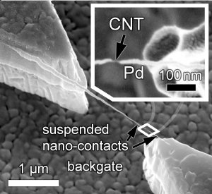 A single carbon nanotube (CNT) is grown between two contacts. The ends were coated by vapour-deposition of palladium to connect to the suspended transistor channel. (Photo: M. Muoth / ETH Zurich)
The limits of conventional microtechnology, based mainly on silicon, have been reached. Smaller and better is achievable only by using new materials and technologies. This is why research hopes for great things from carbon nanotubes (CNTs), ultra-tiny tubules a few nanometres in diameter, made of pure carbon. CNTs have remarkable structural, mechanical and electronic properties. The research group led by Christofer Hierold, Professor of Micro and Nanosystems at ETH Zurich, aims to use these in nano-electronics components. He and his research group, in particular the doctoral student Matthias Muoth, have now succeeded in constructing a hysteresis-free field effect transistor based on an individual CNT with metallic nano-contacts. The researchers reported this recently in “Nature Nanotechnology”.
A nanotube grows
To build the transistor, the researchers allowed a single CNT to grow between two polysilicon tips. For good electrical contact, they vapour-deposited palladium metal onto the ends of the tubule in a highly precise manner. The scientists included a sliding cover, the shadow mask, to protect the midsection of the CNT from unwanted metallization. A silicon substrate, also coated with metal and positioned three microns below the CNT, acted as a control terminal called gate.
The successful fabrication of the transistor with the CNT and the precise interfacing of its ends with palladium are not the only decisive aspects for Christofer Hierold. He considers the breakthrough to be the fact that the transistor does not display what is called gate hysteresis. Hysteresis is absent even at an atmospheric humidity of 45 percent. He regards this as “a considerable step forward for components intended for use as sensors.”
A high-quality arrangement
Hysteresis represents unwanted properties of an electronic system. For example, if the voltage at the transistor’s control gate is increased and then reduced again, there can be an unwanted shift in the transistor’s threshold voltage. The properties of the transistor at a working point then depend on its history, for example on the gate voltages it has been previously exposed to. These undesired shifts in the threshold voltage also originate from charges that can be trapped on defects in the CNT or in oxides in their vicinity.
Such hysteresis is not observed and the researchers regard this as a sign of a particularly high-quality transistor arrangement with low-defect, high-purity CNTs.
Innovative sensors and filters
The new component opens up interesting application possibilities for sensors and other nano-electromechanical components. For example the transistor could be used in highly sensitive gas sensors or strain gauges, and also in a resonator arrangement as a nano-balance. CNT transistors could also be very useful as filters to receive the correct frequency in mobile phones, since they are smaller and use less energy than conventional frequency filters. This involves using electromechanical excitation to cause a CNT with a characteristic frequency to vibrate like a guitar string. All other frequencies, on the other hand, are unable to excite the nanotube. According to the ETH professor, “It is hoped that such nano-electromechanical filters will be better than purely electronic ones.” He says that, in any case, one big advantage of the new components is their low energy demand.
Hierold says that the miniaturisation of the transistor is not yet complete. Only the CNT as a nano-structure with a diameter of one to three nanometres and, as shown here, with channel lengths as short as 30 nanometres and possibly less has been “miniaturised”. The Professor stresses that “We are still using conventional technology for structuring the tips and the shadow mask of the new component.”
A big step forward
The new technology has not yet progressed to the point where it would soon replace transistors of the kind used in present-day computer chips. However, Hierold emphasises that “We have now created a component that allows us to take a big step forwards, especially in micro- and nanosystems technology, i.e. in the area of integrated functional materials for sensors and actuators.”