| Diffractive optical elements, optoelectronic transducers and photonic components, which play an important role in optical data communication, can be substantially improved by lateral nanostructures. With the development of lateral optoelectronic nanostructures the way to controllable diffractive optics is paved. For this, elements with specific interference structures are necessary, which act as specific and possibly controllable transmission or reflection filters. Nanostructured optoelectronic components (e.g. quantum well or quantum dot lasers, photonic crystals) offer large market potentials in the future, e.g. for optical data communication or in the range of consumer electronics (for example laser television). Space Applications that Will Use Nanostructured Optoelectronic Components Nanostructured optoelectronic components offer promising application in space in the fields of optical satellite telecommunications or sensor technology (infrared sensors, high resolution charge-coupled devices, etc). With optical wireless data links (OWL) for intrasatellite communication as well as optical intersatellite links, significantly smaller and lighter devices a higher bandwidth could be realized in comparison to conventional microwave communications. Optical intersatellite links were demonstrated in the frame of the ARTEMIS mission of the ESA. For the data transmission, extreme frequency-stable solid state lasers (Nd:YAG lasers) are used, which are pumped with diode lasers. How Laser Terminals Can Be Used in Scientific Applications The German company, Tesat, is a leading manufacturer of laser terminals for optical intersatellite communication. Such laser terminals are also interesting for scientific applications; for example, as an injection seeder for a satellite-based Doppler-Lidar (ALADDIN), as a satellite-based measuring device for gravitation wave detectors (LISA, with SMART as demonstration mission), or as a frequency normal for a satellite-based FT-spectrometer (POISON). Benefits of Using Quantum Dot (QD) Lasers Semiconductor quantum dots, which have been manufactured in high quality by means of self-organization for about the last 5 years, offer a new degree of freedom in selecting the working wavelength of photonic elements. They allow manufacturers to cover almost completely the entire spectral region from the ultraviolet to the far infrared, with a small number of substrate materials. Further advantages of quantum dot lasers are a small energy consumption through low threshold current densities, a high modulation range for high-speed applications as well as an improved temperature stability. Figure 1 represents the threshold current densities of different types of semiconductor diode lasers. | | | Figure 1. Comparison of threshold current densities of different semiconductor lasers. | Predicted Timescale for Commercial Use of Quantum Dot Lasers Beyond that, an improved radiation hardness has already been proven by quantum dot lasers compared with quantum well lasers. First commercial uses of quantum dot lasers are expected in 2003. Figure 2 shows the schematic structure of a quantum dot Vertical Cavity Surface-Emitting Quantum Dot laser (VCSEL). | 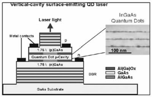
| | Figure 2. Schematic structure of a QD Vertical Cavity Surface Emitting Laser (VCSEL). | What Quantum Dot Lasers Can Be Used for in Space Applications Due to their radiation hardness and the low energy consumption, quantum dot lasers in principle are relevant for space applications, e.g. as pump lasers for solid state lasers, which are needed for different applications. In order to realize the potential of quantum dot lasers in space applications, appropriate measures have to be accomplished by the space industry for the specification, system integration and space qualification. Photonic Crystals Photonic crystals are a further example of nano-optoelectronic components with application potential in optical data communication. Photonic crystals exhibit a periodic refractive index and possess an analogy to semiconductors in electronics, a “photonic band gap” for certain frequency in the visible and IR wavelength ranges. The lattice constant of photonic crystals lies in the range of half the wavelength of the light in the medium. For visible light this means that for the production of photonic crystals, a precision within the range of 10 nm is necessary. Two-dimensional structures today can be routinely manufactured with high precision. Developing Three-Dimensional Photonic Crystals At present, intensified efforts are made for the development of three-dimensional photonic crystals, e.g. with utilization of lithography and self-organization procedures, in which nanoscale colloids (e.g. from polymers or silicates) arrange spontaneously to a cubic lattice. These lattices are used as templates for lattices from more interesting materials such as metals and metal oxides. Three-dimensional photonic crystals would open up new possibilities in optical data communication (light could be guided and branched to arbitrary directions) and offer in principle the potential for the realization of purely optical circuits (optical computing). Such photonic transistors are however at present still very far from realization. In the long run, photonic crystals will find applications in optical satellite communications. Potential Space Applications for Infra-Red Sensors IR sensors offer a multiplicity of application potential in space, e.g. for the satellite-based earth observation and atmosphere research, for astronomy, as navigation aid for space systems or for optical data communication. Approaches for the miniaturization and further improvement of infrared sensors are based among other things on the application of two- (quantum well), one- (quantum wire) or zero-dimensional (quantum dot) nanostructures. With the help of quantum well or quantum dot structures the detection characteristics of IR sensors can be adjusted selectively to the relevant spectral region (band gap engineering). Quantum well IR sensors, based on GaAs are developed, for example, by the Center for Space Microelectronics Technology of NASA for special space applications. This quantum well infrared photodetector (QWIP) consists of a GaAs-layer, which is embedded, sandwich-like, in two AlxGa1-xAs layers. The characteristics of the quantum wells can be adjusted by varying the thickness of the GaAs layer and the composition of the barrier layer. By means of molecular beam epitaxy, nm-thick layers can be produced on large areas with atomic precision. Ga-As QWIP can also be used for long-wave IR radiation > 6 µm. Optimising Infra-Red Sensors with Si/Ge Quantum Dots The Technical University of Munich pursues a different approach in the frame of a BMBF (Bundesministerium für Bildung und Forschung - Federal Ministry of Education and Research) joint project on the self organization of Si/Ge islands on silicon. The research activities are focused on controlling the characteristics of epitactical, defect-free Si/Ge islands on silicon substrates, which can be produced with the self-organizing, parallel Stranski-Krastanow procedure in the material system Si/SiGe. The objective here is to develop coupled systems with several layers of quantum dots in a homogeneous layer system, which exhibit new functions by charge transfer and electrostatic coupling and can be used as optical detectors particularly in the mid IR (MIR) range. With combined QD/QW structures a 50-fold increased photoresponse can be obtained compared with sole quantum dot structures. Expected advantages of QD MIR (mid-infrared) detectors to be mentioned are the extended spectral range, a high durability and reproducibility, radiation hardness and a low dark current. For the year 2003, the realization of a prototype 2-colour IR detector in co-operation with DaimlerChrysler is planned. Note: A complete list of references can be found by referring to the original text. |