| Scanning Probe Microscopy (SPM) is a powerful technique for studying surfaces and surface properties with resolution in the nanometre range. SPM techniques (SPMs) are a group of different instruments characterized by the type of interaction used in the study of surface: • STM (Scanning Tunneling Microscopy), • AFM (Atomic Force Microscopy), • LFM (Lateral Force Microscopy), • MFM (Magnetic Force Microscopy). Scanning Tunneling Microscopy (STM) The Scanning Tunneling Microscopy (STM) was the first technique; in fact, it was invented in 1981 by Gerd Binnig and Heinrich Rohrer at IBM Zurich and after five years they won Nobel Prize in physics. Some years after, Atomic Force Microscopy (AFM) was invented. All the techniques have the components reported in figure 1. | | | Figure 1. Depiction of Scanning Probe Microscopy (SPM) components. | | | | Figure 2. Raster movement. The tip moves on the surface following a precise movement called raster, as shown. | Obtaining Real Image with Atomic Resolution by Using Scanning Tunneling Microscopes (STM) The importance of the STM technique consists in the possibility of acquiring real image with atomic resolution. When the conductive tip is brought within 10 Å from the sample and when a bias voltage (from 1 mW to 1 V) is applied, a tunneling current results depending on the distance of the tip-sample. This signal varies with tip-sample spacing and creates the image because it registers the interaction tip-surface state’s density. Electronic Wave Functions, Tunneling Current and Fermi Levels Both the tip and the sample must be conductive. If the tip-sample distance is in the nanometre range, the electronic wave functions give overlap so the electrons can cross the potential barrier, so we can register tunneling current. In balance conditions the resultant current will be zero, because the flux towards two directions will be equal. The Fermi levels coincide. In figure 3, we report the energy diagram vs. distance, if we apply a bias voltage. | 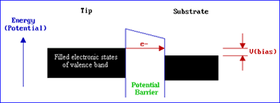
| | Figure 3. Schematic energy vs. distance. | The Two Methods Used to Calculate Tunneling The scientific literature reports two different approaches in order to calculate the tunneling: 1. According to Sommerfeld and Bethe, we can consider the penetration probability of the electronic wave function. 2. According to Bardeen, instead, the tunneling current results as the overlap of electronic states for both the barrier sides (the effective transfer-Hamiltonian). Both methods show how the current density IT depends on the potential's height (or work function), barriers widths and voltage V. Height-Constant Mode and Current-Constant Mode We can operate in height-constant mode or in current-constant mode. In height-constant mode the tip scans sample surface so the tunneling current varies depending on morphology. This mode is faster but acquires significant information only for smooth surfaces. In current-constant mode, instead, the bias is constant and the scanner moves up or down. The motion of the scanner requires more time but the image registers surface details. | 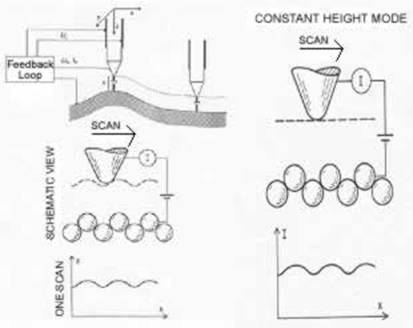
| | Figure 4. The two Scanning Tunneling Microscopy (STM) modes. | Atomic Force Microscopy (AFM) In AFM mode the tip is put on the end of a cantilever, which bends in response to the force between the tip and the sample. The tip is a few microns long and with a diameter of 100Å. The cantilever is long, some hundreds of microns. The deflections due to tip-sample force are detected by a 4-segment photodiode. In this case, is not necessary the tip or the sample be conductive so we can study a lot of sample. Different Modes of Operation for Atomic Force Microscopy (AFM) The AFM can operate in different modes. Contact Mode In which the tip is in contact with the sample. In this case we can work in: 1. Height-constant mode, 2. Force-constant mode. Non-Contact Mode In which the tip doesn’t arrive at the sample surface and is very useful in studying quite fragile or liquid or biological samples. Overall, we use this technique for resist-coated samples. Tapping Mode That is, a combination of the two previous modes. The contact is intermittent because the cantilever end oscillates with such amplitude that the tip touches the sample. Interaction by Van der Waals Forces and the Lennard-Jones Equation If we put the tip close to the sample (distance ≤ 1 nm), we can observe they interact through Van der Waals forces. The resultant force is described by Lennard-Jones equation, i.e. the interaction potential between two electrically neuter and not-magnetic point-like objects: U (r)= -U0 [(r0 / z)12 - (r0 / z)6] U0 = energy in balance conditions, r0 = interatomic distance in balance conditions, z = effective interatomic distance. Figure 5 shows the total force vs. distance tip-sample, and underlines the ranges used for contact or non-contact mode. | 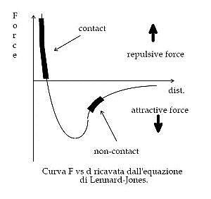
| | Figure 5. Force vs. distance and relative zone modes. | Scanning Probe Microscopy (SPM) Lithography and Nanolithography What the Nobel Prize Richard Feynman hypothesized about the possibility of building condensed matter beginning from elementary bricks, i.e. atoms, it approaches to realty with STM invention. In fact, the nanotechnologies seem to be the realization oh this hypothesis. Our interest is overall focused on nanolithography. Scanning Tunneling Microscopy (STM) Lithography STM lithography is obtained applying tension in the range of some volts. It is possible to bank or remove matter, even in atomic quantities, according to the voltage verse. STM lithography can also remove atoms supplying tension impulses. Atomic Force Microscopy (AFM) Lithography AFM lithography can be obtained using conductive tips and sample in order to produce nano-oxidation or electrical phenomena. AFM lithography, without using potential difference, can be produced applying metal cantilevers with diamond tips. These are scratching and indentation techniques. |