In the late 90s, the concept of building a quantum computer from creating semiconducting silicon components to use as qubits was put forward. Since then, many advances have been made in this field, and scientists have become more in control over the charge and spins in single dopants, pushing forward our expertise in the nanofabrication of semiconductors.
ImageCredit/Shutterstock: Macrophoto
One major barrier has remained, and that is that researchers have continued to be challenged over how to control the exchange interactions and tunneling between two donors. The degeneracy in the conduction band of silicon induces unusual, peculiar oscillatory behavior, as the relative locations of the dopants vary at the scale of the lattice parameter.
In 2018, an international team of researchers in Spain and Brazil proposed that this problem could be overcome by using two-dimensional (2D) materials as semiconductors. The researchers recognized that 2D semiconductors offer benefits that allow them to be easily positioned and manipulated. Further to this, they concluded that many 2D materials have a conduction band minimum at k = 0, resulting in the absence of exchange or tunnel coupling oscillations that are characteristically problematic with silicon.
The team investigated 2D semiconductor materials that were currently available, noting their characteristics and properties, and concluding the practicability of using these 2D materials for semiconductors in qubits, enabling quantum computing. The results of the study uncovered that 2D semiconductors are at least as effective, and possibly more so than the materials currently used in qubits.
2D to replace silicon
Published in the Beilstein J Nanotechnology, the paper proposed a new theory to designing semiconductor materials. Instead of relying on bulk silicon as a host material, as has been the standard protocol, the team put forward an alternative method that replaced the reliance on bulk silicon with 2D semiconductor materials. They suggested that in comparison to using a bulk material, positioning of donors on a surface would be easier because control over just two coordinates is required, eliminating the need for control over the third-dimensional z-component, which adds uncertainties. What’s more, the team figured out that the conduction band minimum presented by numerous 2D materials was at the gamma point, the center of the Brillouin zone. Meaning that the required donor positioning accuracy is reduced as there are no oscillatory exchange and tunnel couplings predicted in this instance.
Why 2D materials?
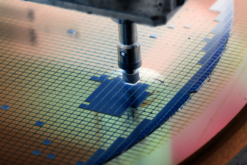
Two-dimensional materials have become the focus of much scientific research over recent years. The materials are made of single layers of atoms, and their special nanoscale properties have found them useful in many applications already including; in renewable energy (photovoltaics), as electrodes, in water purification, and as semiconductors.
The research
The effective mass approach (EMA) approach was decided to be suitable for characterizing the shallow states in semiconductors. The Spanish/Brazilian team analyzed the stability of bound states of single dopants in a 2D semiconductor host, as well as looking at the coupling between pairs of donors in this material, using this approach. To use this method, the researchers had to ensure that the bandgap energy of the material was considerably larger than the binding energies. To achieve this, the unknown dielectric constant was considered as a free parameter, and its minimum value required for the binding energy to fulfill the condition was estimated as a function of the band-gap energy and the effective mass on the conduction band.
The future of qubits and quantum computing
The team was able to prove that there is a potential use for 2D materials as host donors where electrons may serve as qubits. Their research highlighted a variability of binding energies as a function of the substrate, chemical composition, and the number of layers, which supports this notion. They also found that the 2D materials they investigated support shallow states with binding energies. This led them to conclude that different 2D materials could be used for different purposes, with those supporting shallower states being used for manipulation and those with deeper states used for storage.
This research opens the avenue to using 2D semiconductors for efficient use of qubits, which will have a major impact on the development of quantum computers. As knowledge of 2D materials continues to grow, and more become isolated and available for research, scientists will be able to develop more efficient qubits, allowing for the development of a scalable quantum computer.
Source:
https://www.ncbi.nlm.nih.gov/pmc/articles/PMC6204835/
Disclaimer: The views expressed here are those of the author expressed in their private capacity and do not necessarily represent the views of AZoM.com Limited T/A AZoNetwork the owner and operator of this website. This disclaimer forms part of the Terms and conditions of use of this website.